—
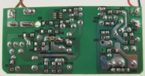
PCB, commonly known as a printed circuit board, is an indispensable component in electronics and plays a crucial role. Throughout the PCB production process, numerous critical factors must be managed. Negligence can lead to defects that impact the entire assembly, leading to persistent quality issues. Therefore, after the circuit board is manufactured, inspection and testing become essential steps. Below are common PCB faults and their solutions.
1. **The PCB board often experiences delamination during use**
**Reasons:**
(1) Issues with supplier materials or processes.
(2) Inadequate selection of materials and copper surface distribution in the design.
(3) Extended storage time, exceeding the recommended period, causing the PCB board to become damp.
(4) Improper packaging or storage leading to moisture exposure.
**Countermeasures:**
Opt for packaging that ensures protection and use constant temperature and humidity control for storage. Conduct thorough PCB reliability tests, such as thermal stress tests. A reliable supplier should meet a standard of more than 5 successful tests without delamination, confirmed during both sample stages and each mass production cycle. Some manufacturers may only require 2 tests and verify them infrequently. Simulated placement IR tests can also help prevent defective products from reaching the market, which is essential for a high-quality PCB manufacturer. Additionally, select PCB boards with a Tg (glass transition temperature) above 145°C for added safety.
**Reliability Testing Equipment:**
– Constant temperature and humidity chamber
– Thermal shock test chamber (stress screening type)
– PCB reliability testing equipment

2. **The solderability of the PCB board is poor**
**Reasons**: Extended storage time leads to moisture absorption, layout contamination and oxidation, abnormal black nickel, solder resist SCUM (shadow), and solder resist PAD.
**Solution**: Adhere strictly to the PCB factory’s quality control plan and maintenance standards during procurement. For instance, with black nickel, verify if the PCB board production plant performs chemical gold out, maintains stable chemical gold wire concentration, conducts frequent analysis, and performs regular gold stripping and phosphorus content tests. Ensure good execution of internal solderability tests.
3. **The PCB board is bent and warped**
**Reasons**: Unreasonable material selection by the supplier, inadequate heavy industry control, improper storage, abnormal operation line, noticeable copper area differences in each layer, and insufficient broken hole production.
**Countermeasures**: Pressurize thin boards with wood pulp boards before packaging to prevent future deformation. If needed, add a fixture to the patch to avoid excessive board bending. Simulate mounting IR conditions for testing before packaging to prevent undesirable bending after the furnace.
4. **PCB board impedance is poor**
**Reason**: Significant impedance variations between PCB batches.
**Countermeasures**: Require the manufacturer to provide batch test reports and impedance strips upon delivery. If necessary, request comparative data on the inner and side wire diameters of the board.
5. **Anti-welding blistering/falling off**
**Reason**: Variations in solder mask ink selection, abnormal PCB solder mask processes, or excessively high patch temperatures.
**Countermeasures**: PCB suppliers should establish reliability test requirements and control them throughout different production processes.
6. **The Avani effect**
**Reason**: During the OSP and Dajinmian processes, electrons dissolve into copper ions, creating a potential difference between gold and copper.
**Countermeasures**: Manufacturers should closely monitor and control the potential difference between gold and copper during production.
**Manufacturing process of multilayer PCB circuit boards**
As electronic products demand increasing functionality, PCB structures are evolving from single-layer to double-layer to multilayer boards. Multilayer PCBs consist of alternating layers of conductive patterns and insulating materials, with more than three layers of conductive patterns. Electrical interconnections between layers are achieved through metallized holes. For instance, using a double-sided board as the inner layer with two single-sided boards as outer layers, or two double-sided boards as inner layers with two single-sided boards as outer layers, results in a four-layer or six-layer PCB, known as a multilayer PCB.
Multilayer PCBs are typically made from epoxy glass cloth copper-clad laminates, with a manufacturing process derived from double-sided boards with plated-through holes. The process begins with etching the inner layer graphics, followed by blackening treatment, adding prepreg for stacking, and placing copper foil on both surfaces. The assembly is then heated and pressed to produce a “double-sided copper-clad laminate” with an inner layer pattern. Following this, numerical control drilling is performed based on the design, and after drilling, the hole walls are etched and de-drilled, leading to the production of the double-sided plated hole printed circuit board.

