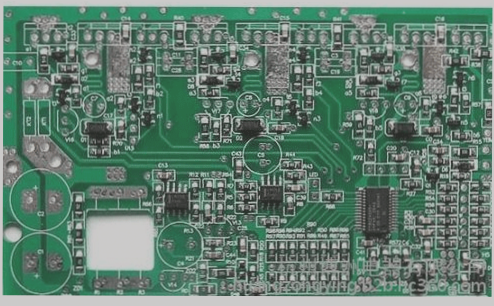
PCBs, commonly known as printed circuit boards, are indispensable components in electronic devices, playing a central role in their functionality. Throughout the series of production processes for PCBs, numerous points must align seamlessly. However, these boards are prone to defects, which can significantly impact the entire PCB assembly, leading to a myriad of quality issues. Consequently, post-manufacture inspection testing becomes an imperative step. Below, we outline some common PCB faults and their corresponding solutions.
Reasons:
(1) Material or process issues from suppliers.
(2) Suboptimal material selection and uneven copper surface distribution in design.
(3) Prolonged storage time, exceeding storage period, or moisture exposure.
(4) Improper packaging or storage methods.
Solutions: Opt for appropriate packaging and utilize constant temperature and humidity control equipment during storage. Implement rigorous reliability testing in PCB factories, such as thermal stress tests as part of the PCB reliability assessment. Some reputable suppliers adhere to a non-layering standard of more than 5 times, verified during sample stages and in each mass production cycle. Conversely, standard manufacturers might only require 2 times, with confirmation occurring every few months. Conducting simulated placement IR tests can further prevent defective products, representing a crucial practice for top-tier PCB factories. Additionally, select PCB boards with a Tg above 145°C for enhanced safety.
Reliability Testing Equipment: Constant temperature and humidity chambers, stress screening thermal shock test chambers, and PCB reliability testing apparatus.
Reasons: Extended storage duration leading to moisture absorption, layout contamination and oxidation, black nickel abnormalities, solder resist SCUM (shadowing), and solder resist PAD issues.
Solutions: Enforce stringent quality control plans and maintenance standards when procuring PCBs. For instance, in cases of black nickel anomalies, verify if the PCB production facility employs chemical gold, maintains stable chemical gold wire concentrations, conducts regular gold stripping and phosphorus content tests, and executes internal solderability tests effectively.
Reasons: Supplier’s material selection inadequacies, lax heavy industry control, improper storage, irregular operation lines, significant discrepancies in copper layer areas, and inadequate broken hole production.
Solutions: Apply pressure to thin boards with wood pulp boards prior to packaging and shipping to prevent future deformation. If necessary, utilize fixtures during assembly to prevent excessive board bending. Conduct IR testing simulating mounting conditions on PCBs before packaging to forestall board bending issues post-furnace.
Reason: Significant impedance differences between PCB batches.
Solution: Manufacturers must provide batch test reports and impedance strips upon delivery. If required, furnish comparative data on inner and outer wire diameters.
Reason: Solder mask issues.
Solution: PCB suppliers should establish reliability testing requirements for PCBs and enforce them across various production stages.
Reason: During OSP, electrons dissolve into copper ions, resulting in a potential difference between gold and copper.
Solution: Manufacturers should closely monitor and control the potential difference between gold and copper during the production process.


