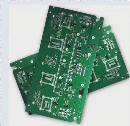
Main Causes and Solutions for Common PCB Printing Issues
-
Bubbles Between Lines:
The narrow line spacing and high lines during screen printing can lead to bubbles due to inadequate adhesion of the solder mask to the substrate. This entrapment of air or moisture causes excessive line elevation and hindered printing. Solution: Ensure complete coverage during printing and control electroplating current.
-
Issues with FPC Boards:
Delays in paper printing can cause residual ink accumulation, leading to irregularities in the solder mask. Inadequate cleanliness during exposure can result in pinholes. Solution: Maintain a timely printing schedule and use high-mesh screens for plate making.
-
Surface Contamination:
Inadequate drying and splashing before solder mask printing can contaminate the board. Solution: Inspect for copper foil oxidation during screen printing.
-
Uneven Surface:
Surface contamination from debris and residual ink accumulation can create an uneven surface. Solution: Maintain cleanliness, restrict non-essential personnel, and remove residual ink diligently during screen printing.
-
Ghosting Issues:
Improper positioning and ink removal can lead to ghosting and cracks on the board. Solution: Fix paper firmly, remove ink promptly, and ensure precise exposure parameters to prevent cracks.


