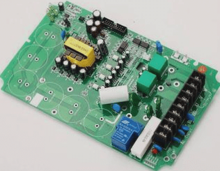
Important Tips for PCB Design
- Single-sided pads must be clearly marked if drilled.
- Utilize filler blocks when drawing pads. While this can pass DRC inspections, it may pose challenges during processing. Solder mask data cannot be directly generated from pads with filler blocks, making component soldering difficult when the solder resist covers the filler block area.
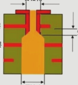
- The electrical ground layer acts as a flower pad and connection. Designers need to be cautious as the ground layer may appear inverted, with connections represented as isolated lines. Care must be taken to avoid gaps that could short-circuit power supplies and block connection areas.
- Define the processing level clearly. For single-sided boards designed on the TOP layer, specifying the front and back is crucial to simplify component soldering during manufacturing. Layer order must be strictly followed in multi-layer boards.
- Avoid excessive filler blocks or thin lines in designs to prevent loss or incompleteness of Gerber data. Drawing filler blocks individually with lines can complicate data processing due to increased data volume.
- Ensure surface mount device pads are of adequate length for proper continuity testing. Short pads may hinder the correct staggering of test pins.
- Maintain a minimum gap of 0.3mm between lines forming large-area grid lines during PCB manufacturing to prevent wire breakage.
- Keep a distance of at least 0.2mm between large-area copper foil and the outer frame to avoid warping and solder resist peeling off during copper foil shaping.
- Clearly define the outline frame to prevent confusion for PCB manufacturers. Overlapping contour lines from different sources can help avoid ambiguity.
- Ensure even PCB graphic design to prevent quality issues during pattern plating.
- Use grid lines when copper areas are large to prevent blistering during Surface Mount Technology (SMT) processes.
These tips are essential for successful PCB design and manufacturing processes. Implementing them will help avoid common pitfalls and ensure the quality and reliability of your printed circuit boards.