### Common Misunderstandings in Differential Signal and PCB Design
Differential signals (Differential Signal) are becoming increasingly prevalent in high-speed circuit design. In fact, the most critical signals in a circuit are often designed using a differential structure. What makes differential signaling so popular? And how can we ensure its optimal performance in PCB design? These are the two key questions we’ll explore in the following discussion.
**What is a differential signal?**
In simple terms, a driving source sends two equal but inverted signals, and the receiving end determines the logical state (either “0” or “1”) by comparing the difference between these two voltages. The pair of traces that carry differential signals is known as differential traces.
Compared to conventional single-ended signal traces, differential signals offer three main advantages:
1. **Enhanced Noise Immunity**
Due to the excellent coupling between the two differential traces, external noise or interference is nearly equally coupled to both lines. The receiver only cares about the voltage difference between the two signals, allowing any common-mode noise to be fully canceled out.
2. **Effective EMI Suppression**
Similarly, because the two signals have opposite polarities, the electromagnetic fields they radiate can cancel each other out. The tighter the coupling between the traces, the less electromagnetic energy is emitted into the surrounding environment.
3. **Accurate Timing and Positioning**
The switch transition in a differential signal occurs at the intersection of the two signals. This is different from conventional single-ended signals, which rely on high and low threshold voltages to determine logic states. As a result, differential signals are less sensitive to process variations and temperature changes, reducing timing errors. Additionally, differential signaling is particularly well-suited for low-amplitude signal circuits, such as those using the popular LVDS (Low-Voltage Differential Signaling) technology.
For PCB engineers, the main concern is how to fully leverage the advantages of differential routing in the actual layout. Those familiar with layout design will likely be aware of the common guideline for differential traces: “equal length and equal spacing.” Equal length ensures that the two differential signals remain in opposite polarity at all times, minimizing the common-mode component; equal spacing is crucial to maintain consistent differential impedance and reduce signal reflections. “As close as possible” is sometimes an additional requirement for differential traces. However, these guidelines should not be applied mechanically without understanding the underlying principles, as many engineers still fail to grasp the essence of high-speed differential signal transmission.
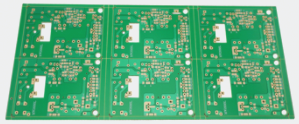
The following addresses several common misconceptions in PCB differential signal design.
Misunderstanding 1: Some believe that differential signals do not require a ground plane as a return path, or that the differential traces themselves provide return paths for each other. This misunderstanding arises from superficial observations or a lack of deep understanding of high-speed signal transmission mechanisms. Differential circuits are generally less sensitive to ground bounces and noise signals on power and ground planes. However, partial return cancellation in the ground plane does not mean the differential circuit does not rely on the reference plane for its return path. In signal return analysis, the principles for differential and single-ended traces are the same: high-frequency signals always flow along the loop with the least inductance. The main difference is that, in addition to coupling with the ground, differential traces also experience mutual coupling. The stronger coupling type determines the main return path. In PCB design, the coupling between differential traces is usually minimal, often just 10-20% of the total coupling, with the majority being to the ground. Therefore, the primary return path for differential signals still lies on the ground plane. When the ground plane is interrupted, the coupling between differential traces in the area lacking a reference plane may provide the main return path. While ground plane discontinuities may not severely affect single-ended traces, they still degrade the quality of differential signals and increase EMI, which should be avoided. Some designers mistakenly think removing the reference plane beneath differential traces can help suppress common-mode signals. However, this approach is theoretically flawed. Not providing a ground return loop for common-mode signals will inevitably cause EMI radiation, doing more harm than good.
Misunderstanding 2: It is thought that maintaining equal spacing is more critical than matching the trace length. In practical PCB layouts, it is often impossible to achieve both spacing and length matching simultaneously. Due to constraints such as pin distribution, vias, and available routing space, achieving length matching often requires winding the traces. As a result, parts of the differential pair may not remain parallel. The most crucial rule for PCB differential trace design is to match the trace lengths, while other rules can be adjusted based on specific design requirements and application needs.
Misunderstanding 3: Some believe that differential traces must be placed very close together. Keeping differential traces close merely increases their mutual coupling, which can enhance noise immunity and reduce electromagnetic interference (EMI) by leveraging opposing magnetic fields. While this is beneficial in many cases, it is not always necessary. If external interference can be effectively shielded, strong coupling may not be required to suppress EMI. To achieve better isolation and shielding for differential traces, one basic method is to increase the spacing between them and other signal traces. The electromagnetic field strength decreases with the square of the distance, so when the trace spacing exceeds four times the trace width, interference becomes negligible. Ground plane isolation can also provide effective shielding, commonly used in high-frequency (above 10G) IC package PCB designs. This approach is known as the CPW structure and helps ensure precise differential impedance control (2Z0). Differential traces can also be routed in different signal layers, but this is generally not recommended, as impedance variations and vias between layers can disrupt differential mode transmission and introduce common-mode noise. Additionally, insufficient coupling between adjacent layers may reduce noise resistance, although maintaining proper distance from surrounding traces can mitigate crosstalk. At typical frequencies (below GHz), EMI is usually not a major concern. Experiments have shown that at 500 mils from a differential trace, the radiated energy is attenuated by 60dB at 3 meters, which is sufficient to meet FCC electromagnetic radiation standards. Thus, designers need not overly worry about electromagnetic interference due to insufficient coupling in differential traces.
If your have any questions about PCB ,please contact me info@wellcircuits.com

