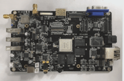
(1) Part packaging refers to the physical appearance and solder pad positions indicated when the actual component is soldered onto the printed circuit board.
(2) Part packaging pertains solely to the component’s physical appearance and solder pad positioning. Purely from a packaging standpoint, different components can share the same part packaging. Conversely, identical components may have various packaging forms; for instance, RES2 signifies a resistor, which can have packaging options like AXIAL0.4, AXIAL0.3, AXIAL0.6, etc. Therefore, when selecting components for soldering, it’s crucial to know not just the component name but also its specific packaging.
(3) The packaging of components can be specified within the circuit diagram design or in the parts list. You can define the footprint settings in the Part Properties dialog during circuit diagram design, or specify the component packaging during the import of the parts list.
—
Question 2: What is the difference between wire, flying wire, and network?
Wire, also known as copper trace, is used to connect each solder joint and is a crucial component in printed circuit boards (PCBs). PCB design revolves around how wires are arranged.
Another type of wire related to conductors is often referred to as flying wires or pre-drawn wires. After the introduction of the network table, the system generates rules which are used to guide wire routing.
There is a fundamental distinction between flying wires and conductive wires. Flying wires only serve as a form of connection between solder joints without electrical significance. Wires are arranged based on the connection relationships indicated by flying wires, which establish electrical connections.
A network differs from a wire in that it encompasses solder joints. Therefore, referencing a network includes not only the wires but also the solder joints they connect.
Question 3: What is the difference between inner layers and middle layers?
Middle layers and inner layers are often confused. The middle layer refers to the intermediate board layer used for wiring, which is where wires are distributed. The inner layer, on the other hand, refers to the power or ground layer, typically without wiring, consisting of a continuous sheet of copper foil.
Question 4: What are internal and external network tables, and how do they differ?
Network tables are categorized as either external or internal. An external network table denotes the schematic network table generated by tools like Sch or other schematic design software. In contrast, an internal network table is derived from the imported external network table after modifications, specifically used in the PCB system for wiring. While these two types of nettables are distinct concepts, readers need not strictly differentiate between them.
Question 5: What is the role of the netlist manager?
The netlist manager facilitates the integration of schematic design data into the PCB design system. Changes in PCB design data are executed using Netlist Macro, automatically generated by comparing and analyzing network table files with internal PCB system data. Additionally, the netlist manager enables direct editing of component connection relationships within the PCB system to create the network table.
Question 6: What is a class, and what are the benefits of introducing it?
A class in PCBs is a grouping of units with similar purposes defined by users themselves. Introducing classes serves two primary purposes:
1. **Facilitating Wiring:** During PCB wiring, certain networks require special handling. For instance, critical data lines might need increased spacing from other components to prevent interference. Grouping these lines into a class allows rules such as spacing constraints to be applied uniformly, enhancing automated wiring efficiency.
2. **Simplifying Component Management:** In large circuit boards with numerous components and networks, classes simplify management. For example, grouping all input networks into a class allows for easier navigation and management when searching for specific components.
Question 7: How can additional solder joints be added to a network?
To add solder joints to a network, first place the solder joint on the circuit board. Then, double-click the solder joint to open the properties dialog box. In the Advanced Net items section, select the appropriate network to complete the solder joint placement.
Question 8: What is the purpose of inner segmentation?
Inner layers can be utilized to connect critical circuits, thereby enhancing anti-interference capabilities and providing protective functions for important circuits.
Question 9: What is the purpose of copper plating, and what precautions should be taken?
Copper plating primarily improves the circuit board’s anti-interference capabilities. When wrapping wires or filling tear drops on lines, ensure proper copper plating on the PCB board.