The Importance of PCB & PCBA Testing in Electronics Manufacturing
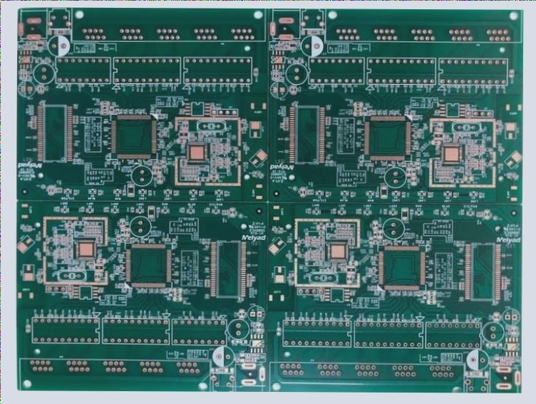
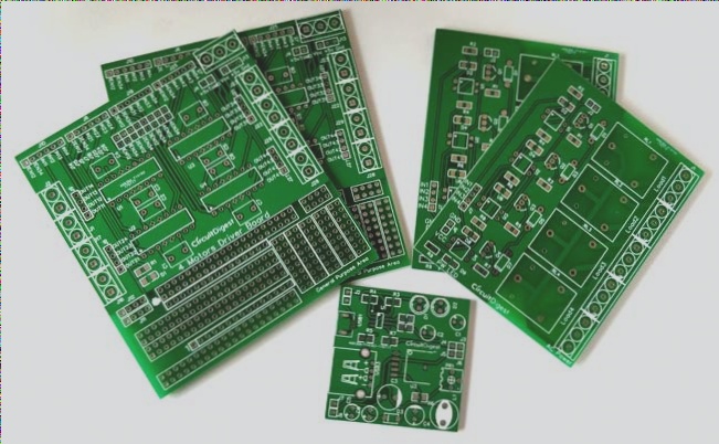
PCBs (Printed Circuit Boards) are crucial for electronic components’ support and electrical interconnection. They are extensively used in Medical Devices, Consumer Electronics, and Industrial Equipment due to their reliability and high density. The demand for PCBs has been rapidly increasing, necessitating stringent quality control measures.
Regardless of the application, PCBs must meet project specifications. Therefore, PCB & PCBA testing is vital during manufacturing to detect any defects that could lead to malfunctions. In this article, we explore common testing techniques used by wellcircuits, a leading PCB & PCBA manufacturer in China.

1. Benefits of PCB & PCBA Testing
Testing PCBs and PCBA early helps identify and rectify critical errors, reducing costs, saving time, and enhancing safety. Screening out defective boards in the initial stages prevents wastage, as rectifying finished products is more challenging and expensive. Detecting defects early in the production process minimizes modification costs.
2. Common Defects to Test for PCB and PCBA
During manufacturing, it’s essential to test for common defects in PCBs and PCB Assemblies:
2.1 For PCB
- Open circuits
- Insufficient connections
- Short circuits
- Missing electrical components
- Misaligned components
Common PCB & PCBA Testing Techniques
1. Defects in Electrical Components
- Defective electrical component
- Wrong component
- Excess solder
- Missing non-electrical component
- Wrong orientation
- Defective non-electrical component
2. Soldering Defects for PCBA
- Open circuits
- Solder bridges
- Solder shorts
- Insufficient solder
- Solder void
- Excess solder
- Solder quality
3. Component Defects for PCBA
- Lifted lead
- Missing component
- Misaligned/misplaced components
- Incorrect component value
- Faulty component
4. BGA and CSP Defects
- BGA shorts
- BGA open circuit connections
Common PCB & PCBA Testing Techniques
3.1 Manual Visual Inspection
Manual visual inspection is a traditional technique using a magnifier or microscope to check the assembled board’s quality visually. It is suitable for simpler boards with fewer components and soldering connections. However, it is prone to human error, missed defects, and lacks consistency in detection. As PCB designs become denser with smaller components, this technique may not be feasible in the long run.
Automated Optical Inspection (AOI)
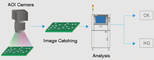
Automated Optical Inspection (AOI) is a crucial testing method for PCBs and PCB assembly. Using high-resolution cameras, AOI automatically scans circuit boards to detect potential defects early on. By comparing captured images with original design files, manufacturers can identify and rectify issues efficiently.
AOI is typically conducted both before and after the solder reflow stage. By addressing any faults during these stages, the cost of rectification is significantly lower compared to post-final testing. To ensure top-notch quality, leading PCB manufacturers like wellcircuits implement AOI multiple times throughout production processes.
Automatic X-ray Inspection (AXI)
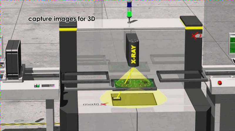
While AOI is adept at detecting various defects, it may struggle with hidden connections and solders, especially in BGA packages. Automatic X-ray Inspection (AXI) was developed to address this limitation. By utilizing X-rays to reveal concealed structures based on different absorption rates, AXI is ideal for inspecting ultra-fine pitch and ultra-high-density circuit boards.
AXI excels in identifying issues like bridges, missing chips, and poor alignments that occur during assembly. Particularly for BGA and solder balls, AXI is indispensable for assessing soldering quality. With the rise of surface mount technology (SMT) and the complexity of modern boards, AXI is witnessing increased adoption in PCB manufacturing, including at wellcircuits for PCB assembly services.
Bed of Nails Testing
Bed of Nails Testing is a traditional electronic test fixture employed post-PCB assembly. This method involves an array of spring-loaded pogo pins aligned to make contact with test points on the circuit board. Connected to a measuring unit, the fixture assesses the assembly’s quality by checking for shorts, opens, resistance, and capacitance.
The testing process, controlled by software, is swift, taking only seconds to test a single board. As it directly contacts test points within the circuitry, individual component testing and performance measurement are accurate. However, the need for specific fixtures for each PCB type can make it costly for prototype testing but remains a viable option for small-batch orders.
3.5 Flying Probe Testing
The flying probe testing method is an advancement from the traditional bed of nails tester. Unlike the bed of nails tester, the flying probe tester eliminates the need for a fixture, reducing costs associated with specific probes and custom tool manufacturing. By utilizing 2 or more movable probes instead of a fixed bed of nails, this testing technique can effectively detect PCBs with high component density and small pitch widths.
Flying probe testing is commonly employed for testing analog components, analog signature analysis, and identifying short/open circuits. While it offers lower initial costs compared to the bed of nails technique, its testing speed is notably slower. This characteristic makes it ideal for testing PCB prototypes and small-batch orders but less efficient for large-scale production. At wellcircuits, all boards undergo flying probe testing before delivery to customers.
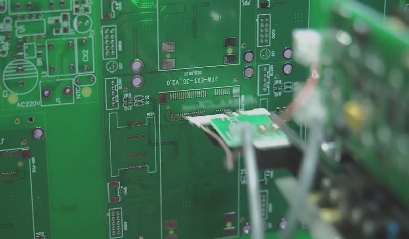
Image courtesy: wellcircuits.com
3.6 Functional Testing
Functional testing, as the name implies, assesses whether assembled PCBs will operate as intended. This testing method simulates the final electrical environment of the PCB to ensure proper functionality and power-up. Typically conducted as the final step in the manufacturing process, functional testing, while complex and costly in terms of testing programs, offers excellent quality assurance.
4. Conclusions
PCB & PCBA testing plays a vital role in the manufacturing process. Early defect detection helps save costs and prevent issues before final production. With component miniaturization and PCB design complexity on the rise, there is a growing demand for advanced testing techniques. Choosing the appropriate tests should align with the quality standards of the boards. While a combination of testing methods can detect most defects, it is crucial to select the most cost-effective solution tailored to specific needs.
Wellcircuits provides all the aforementioned testing services and is equipped with skilled engineers and technicians ready to support your PCB and PCBA orders. They offer expert guidance and can be your reliable partner for upcoming PCB projects.

