The PCB Tin Sinking Process
The PCB tin sinking process is a specialized technique aimed at improving surface mount technology (SMT) and chip packaging. It involves chemically depositing a tin metal coating onto the copper surface, replacing the traditional Pb-Sn alloy coating method. This innovative and eco-friendly process is extensively used in electronic products, hardware, decorations, and more.
Tin Spraying vs. Tin Sinking
- Tin Spraying: This process immerses the PCB into molten tin paste, creating a dense tin layer ranging from 1µm to 40µm. The sprayed tin is pure and easy to clean, with a long shelf life and high resistance to scratching.
- Tin Sinking: In contrast, tin immersion creates a thinner tin layer of about 0.8µm to 1.2µm. It has a looser structure, lower hardness, and is more prone to scratching and discoloration during welding. The immersion tin process involves complex chemical reactions, making cleaning challenging.
Chemical Tin Deposition
Chemical tin deposition is a widely used method in PCB manufacturing. It alters the chemical potential of copper ions, leading to a chemical substitution reaction with stannous ions in the plating solution. This electrochemical process deposits tin onto the copper substrate, forming a tin plating layer.
Common Defects in Tin Immersion Plates
Darkened tin surfaces and poor solderability are common issues in chemical tin immersion plates, often caused by surface contamination. Factors contributing to these defects include liquid consumption during production, improper baking time, and inadequate cleaning processes.
Comparison Between Tin Spraying and Tin Sinking
- Similarities: Both processes are used for lead-free soldering surface treatment.
- Differences:
- Process Flow: Tin spraying involves pre-treatment, tin spraying, testing, molding, and appearance inspection. Tin sinking follows testing, chemical treatment, tin immersion, molding, and appearance inspection.
- Process Principle: Tin spraying directly immerses the PCB in molten tin paste to create a dense tin layer, while tin immersion relies on a displacement reaction to form a thinner tin layer on the surface.
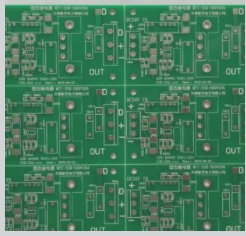
Physical Characteristics of Spray Tin vs. Immersion Tin
- Spray tin typically has a tin layer thickness ranging from 1 µm to 40 µm, with a dense surface structure and higher hardness.
- It uses pure tin during production, making it easy to clean and resistant to scratches.
- Spray tin can be stored for up to one year at normal temperatures without significant discoloration during welding.
- On the other hand, immersion tin has a thickness of about 0.8 µm to 1.2 µm, a looser surface structure, lower hardness, and is more susceptible to scratches.
- Cleaning immersion tin is challenging due to complex chemical reactions, and residues can cause color variations during welding.
- Immersion tin has a shorter storage duration of three months at room temperature, with a higher risk of discoloration over time.
Appearance Characteristics of Spray Tin vs. Immersion Tin
- Spray tin boasts a bright and attractive surface finish.
- In contrast, immersion tin has a light white, dull surface that is prone to discoloration.

