Types of PCB Electroplating Techniques
-
Gold Plating of the Entire Board
Gold plating methods such as electroplated gold, electroplated nickel-gold, electrolytic gold, electric gold, and electric nickel-gold involve dissolving nickel and gold salts in a chemical solution. The PCB is then immersed in an electroplating tank, and current is passed through to form a nickel-gold coating on the copper traces.
Soft gold and hard gold are two common types of gold plating used in PCBs. Soft gold is ideal for general applications, while hard gold is preferred for durable applications like gold fingers, which are connectors on PCB edges.
-
Immersion Plating
Immersion plating deposits a metal layer on the PCB through a chemical reaction, without the use of electric current. This process, also known as immersion gold plating, creates a thicker metal layer and offers excellent corrosion resistance.
Unlike electroplating, immersion plating chemically deposits the gold layer by immersing the PCB in a solution containing gold salt, making it suitable for applications requiring thicker gold coatings.
-
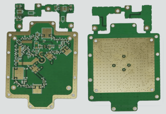
Gold-Plated PCBs
Gold-plated boards provide advantages in managing denser IC connections, particularly for Surface-Mount Technology (SMT) applications with high pin densities. Gold plating offers enhanced pad flatness for better solder paste printing quality and longer shelf life compared to tin-sprayed boards.
In high-density and ultra-small surface mount applications, gold plating’s superior pad flatness is crucial, making it a popular choice for complex circuit designs.
Signal Integrity Considerations in High-Frequency PCB Designs
- At higher frequencies, the skin effect can impact signal transmission in multi-layer PCBs.
- Skin depth, influenced by frequency, is a critical factor in signal integrity.
Comparison: Immersion Gold vs. Gold-Plated Boards
Immersion gold technology offers advantages over traditional gold-plated PCBs:
- Improved Aesthetic and Performance: Immersion gold provides a uniform appearance and enhanced board performance.
- Enhanced Soldering Properties: Easier soldering process reduces the risk of poor solder joints.
- Signal Integrity and Skin Effect: Minimizes skin effect impact on signal transmission in high frequencies.
- Resistance to Oxidation: Denser crystal structure enhances oxidation resistance for long-lasting performance.
- Reduced Risk of Short Circuits: Lower risk of short circuits due to the thin gold layer on pads.
- Improved Adhesion: Robust interface between solder mask and copper layer for better adhesion.
- Enhanced PCB Processing: Consistent results in production runs with less impact from adjustments.
- Stress Control for Bonding: Easier stress control for bonding applications, suitable for chip bonding.
- Flatness and Shelf Life: Offers similar benefits to gold-plated boards for long-term applications.
Conclusion
Both gold-plated and immersion gold boards play essential roles in PCB manufacturing:
- Gold-plated boards excel in flatness and shelf life during prototyping.
- Immersion gold boards offer improved solderability, signal transmission, and reduced risk of oxidation and short circuits.
Engineers can choose based on project needs, considering cost, performance, and reliability.