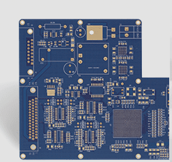
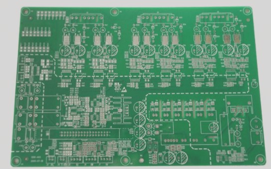
Via (via), also known as metalized holes, is a critical component in PCB design. In double-sided and multi-layer boards, vias are drilled at the intersections of traces that need to connect between different layers. There are three main types of vias: blind vias, buried vias, and through vias. In this article, Banermei has compiled some common questions and answers about PCB “vias,” which we hope will be helpful to you.
1. I often see many holes on a PCB. Does having more vias improve the design? Are there any guidelines?
Answer: No. The use of vias should be minimized, and when vias are necessary, efforts should be made to reduce their impact on the circuit’s performance.
2. In the board layout, if the traces are dense, there may be more vias. Naturally, this will affect the electrical performance of the board. How can I improve the board’s electrical performance?
Answer: For low-frequency signals, vias are less of a concern. However, for high-frequency signals, it’s best to minimize the number of vias. If there are many traces, consider using multi-layer boards to reduce the need for vias.

3. **How do through holes and blind holes affect signal integrity? What are the underlying principles?**
Answer: Blind vias or buried vias are effective solutions for increasing the density of multilayer PCBs, reducing both the number of layers and board size, while significantly decreasing the reliance on plated through holes. However, through holes are simpler to implement and more cost-effective, which is why they are commonly used in designs.
4. **Can you explain the relationship between line width and via size in impedance matching?**
Answer: There isn’t a simple proportional relationship between line width and via size, as the simulations for each are based on different principles. Line width pertains to surface transmission, while via size relates to ring transmission. To achieve proper impedance matching, you can use via impedance calculation software available online, ensuring that the via impedance aligns with the impedance of the transmission line.
5. **What is the relationship between line width, via size on the PCB, and the current-carrying capacity?**
Answer: Typically, a 1-ounce copper PCB has a thickness of about 1.4 mils, and a line width of around 1 mil can carry roughly 1A of current. The situation for vias is more complex. In addition to the via pad size, the thickness of the electroplated copper on the via wall also plays a role in determining the current-carrying capacity.
6. **Should the impedance characteristic Sqrt(L/C) be matched to the via holes?**
Answer: Yes, this is a form of impedance matching. The via parameters should be adjusted to ensure a smooth transition of impedance, which minimizes signal reflection and loss.
7. **Is there a correlation between temperature changes and via impedance?**
Answer: Temperature variations primarily affect the reliability of the vias, rather than their impedance directly. When selecting materials, it is essential to consider the Coefficient of Thermal Expansion (CTE) to account for the effects of thermal expansion and contraction.
8. **How should vias be managed in high-speed PCB routing? Any suggestions?**
Answer: For high-speed PCBs, it’s advisable to minimize the use of vias. Instead, increase the number of signal layers to reduce the need for additional vias, which can introduce signal integrity issues and increase path inductance.
9. **What is the purpose and principle behind adding ground vias near signal vias?**
Answer: PCB vias serve various functions and can be classified as follows:
1) Signal vias (where the via structure has minimal impact on signal integrity)
2) Power and ground vias (where the via structure should minimize the distributed inductance)
3) Thermal vias (where the via structure should minimize thermal resistance)
The addition of a ground via near a signal via helps provide the shortest return path for the signal. Since a signal via represents an impedance discontinuity, the return path can be disrupted. By adding grounding vias around the signal via, the return path is shortened, reducing signal radiation and minimizing electromagnetic interference (EMI). This is especially important at higher frequencies, where EMI increases significantly.
10. **If the signal via hole diameter is small (e.g., 0.3mm), could the via metallization be insufficient?**
Answer: If the via hole is small and deep (i.e., with a relatively large aspect ratio), it may indeed experience incomplete metallization, leading to poor electrical performance.
If you have any PCB manufacturing needs, please do not hesitate to contact me.Contact me
1. I often see many holes on a PCB. Does having more vias improve the design? Are there any guidelines?
Answer: No. The use of vias should be minimized, and when vias are necessary, efforts should be made to reduce their impact on the circuit’s performance.
2. In the board layout, if the traces are dense, there may be more vias. Naturally, this will affect the electrical performance of the board. How can I improve the board’s electrical performance?
Answer: For low-frequency signals, vias are less of a concern. However, for high-frequency signals, it’s best to minimize the number of vias. If there are many traces, consider using multi-layer boards to reduce the need for vias.

3. **How do through holes and blind holes affect signal integrity? What are the underlying principles?**
Answer: Blind vias or buried vias are effective solutions for increasing the density of multilayer PCBs, reducing both the number of layers and board size, while significantly decreasing the reliance on plated through holes. However, through holes are simpler to implement and more cost-effective, which is why they are commonly used in designs.
4. **Can you explain the relationship between line width and via size in impedance matching?**
Answer: There isn’t a simple proportional relationship between line width and via size, as the simulations for each are based on different principles. Line width pertains to surface transmission, while via size relates to ring transmission. To achieve proper impedance matching, you can use via impedance calculation software available online, ensuring that the via impedance aligns with the impedance of the transmission line.
5. **What is the relationship between line width, via size on the PCB, and the current-carrying capacity?**
Answer: Typically, a 1-ounce copper PCB has a thickness of about 1.4 mils, and a line width of around 1 mil can carry roughly 1A of current. The situation for vias is more complex. In addition to the via pad size, the thickness of the electroplated copper on the via wall also plays a role in determining the current-carrying capacity.
6. **Should the impedance characteristic Sqrt(L/C) be matched to the via holes?**
Answer: Yes, this is a form of impedance matching. The via parameters should be adjusted to ensure a smooth transition of impedance, which minimizes signal reflection and loss.
7. **Is there a correlation between temperature changes and via impedance?**
Answer: Temperature variations primarily affect the reliability of the vias, rather than their impedance directly. When selecting materials, it is essential to consider the Coefficient of Thermal Expansion (CTE) to account for the effects of thermal expansion and contraction.
8. **How should vias be managed in high-speed PCB routing? Any suggestions?**
Answer: For high-speed PCBs, it’s advisable to minimize the use of vias. Instead, increase the number of signal layers to reduce the need for additional vias, which can introduce signal integrity issues and increase path inductance.
9. **What is the purpose and principle behind adding ground vias near signal vias?**
Answer: PCB vias serve various functions and can be classified as follows:
1) Signal vias (where the via structure has minimal impact on signal integrity)
2) Power and ground vias (where the via structure should minimize the distributed inductance)
3) Thermal vias (where the via structure should minimize thermal resistance)
The addition of a ground via near a signal via helps provide the shortest return path for the signal. Since a signal via represents an impedance discontinuity, the return path can be disrupted. By adding grounding vias around the signal via, the return path is shortened, reducing signal radiation and minimizing electromagnetic interference (EMI). This is especially important at higher frequencies, where EMI increases significantly.
10. **If the signal via hole diameter is small (e.g., 0.3mm), could the via metallization be insufficient?**
Answer: If the via hole is small and deep (i.e., with a relatively large aspect ratio), it may indeed experience incomplete metallization, leading to poor electrical performance.
If you have any PCB manufacturing needs, please do not hesitate to contact me.Contact me


