1. The relationship between the drop of the component and the thickness of the gold plating on the circuit board.
2. The gold plating thickness on the PCB is specified. After SMT assembly, an issue of component detachment was observed. Initially, the PCB factory strongly believed this was due to black pad formation. The solder pads displayed black pad characteristics, and most of the solder pads connected to the component leads were falling off.
3. In reality, the PCB company’s products are outsourced to specialized OEMs, which are responsible for production quality. However, many uncertainties arise in outsourcing operations, particularly regarding liability ownership and compensation.
4. When the SMT foundry and the circuit board manufacturer exchanged accusations over several rounds, the focus turned to the black pad issue. EDX/SEM analysis was conducted on the samples, revealing that phosphorus (P) content was considered excessively high. They claimed to have performed their own EDX/SEM analysis, asserting that phosphorus (P) levels fell within normal limits.
5. It was noted that the gold-plated layer was too thin, measuring less than 1.0µ”. There are claims that a thin gold layer is ineffective for soldering. However, has anyone truly conducted a slicing analysis to determine at which level the component is detaching? Is the intermetallic compound (IMC) growth insufficient? Could inadequate temperature during soldering be causing poor connections? Is the oxidation of the nickel layer (EN, Electroless Nickel) compromising the solder joint strength?
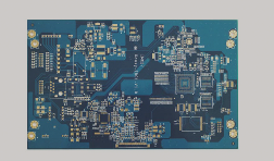
1. After receiving the PCB company’s goods that could not be shipped, I ultimately had to intervene for arbitration and gather all relevant parties for a meeting!
2. First, it is crucial to assess the current situation. We must confirm that the part failures only occur during the box build of the final product, as parts need to be plugged and unplugged during the complete assembly. No issues were detected during the prior SMT and ICT processes.
3. Moreover, upon examining the circuit board assemblies with both working and non-working components, it was discovered that the functional circuit board parts can withstand a thrust of 6-8 Kg-f without detaching, while the defective ones fail under just 2 Kg-f.
4. Therefore, as an immediate measure, we can initially use thrust testing to differentiate between good and defective products; however, parts that have been thrust-tested must be hand-soldered again to ensure that no minor solder joint cracks were caused during this process.
5. As for the assembly of the finished product, this is indeed a challenge. We ultimately decided to conduct a 100% plug-in test on the last batch of products in our warehouse, followed by disassembly based on AQL 0.4 to check the thrust on the parts. For other batches, we will use the pallet as a unit, conducting a 100% plug-in test and selecting two sets for thrust testing. This is a significant undertaking!
6. Next, we will delve into the root causes of part failures. The falling parts can be attributed to several potential issues. First, we should identify where the parts are failing to pinpoint the problem:
7. ▪ If there is no solder on the component leads, it could be due to oxidation of the leads or poor solder paste quality.
8. ▪ If there is no growth into the IMC at all, this may indicate insufficient reflow heat.
9. ▪ If the fracture is located on the surface of the IMC layer, we need to determine whether there are issues with IMC growth. If design factors are not at fault and IMC growth is suboptimal, it may result from inadequate reflow temperatures.
10. ▪ If fractures occur between the IMC and the nickel layer, we should examine whether the phosphorus-rich layer is prominent. Elemental analysis is advisable to assess phosphorus content; excessive thickness may compromise future reliability and structural integrity, and could also result from nickel layer oxidation affecting solder strength.
11. Taking the problematic board, we should slice the solder pads where parts have fallen off and compare them to pads where parts remain intact. Additionally, we should analyze another previously produced, problem-free board to inspect the pads where failures have occurred.
12. The image illustrates a problematic board alongside a sliced section showing the fallen solder pad.
13. It is evident that the IMC of the pads where components fell off appears to be incompletely developed, suggesting potential retention issues with AuSn and AuSn2 (elemental composition remains uncertain).
14. A biopsy analysis of the areas where parts detached also indicated normal IMC.
15. After several days of investigation and discussion, we seem to be unraveling the truth. It appears that part failures are occurring between the IMC and the nickel layer, with IMC growth appearing somewhat inadequate. Both parties have identified oxygen presence in the nickel layer.
16. One party maintains that nickel layer corrosion (Ni erosion) may be a factor, while the other insists that it stems from nickel oxidation (Ni oxidation). Although there is a sense that the PCB manufacturer has not disclosed the complete truth, they have at least acknowledged some issues in their manufacturing process and found flaws in managing a specific gold slot, agreeing to absorb the losses, so we will not pursue further complaints.
17. The distinction between nickel erosion and oxidation seems to revolve around the control of gold layer thickness. Perhaps Shenzhen Honglijie’s understanding requires further refinement!
18. The opinions from Shenzhen Honglijie may serve as a reference. Circuit board experts are encouraged to provide feedback. According to IPC4552, the recommended thickness for the gold layer ranges from 2µ” to 5µ”, while the chemical nickel layer should be between 3µm (118µ”) and 6µm (236µ”).
19. However, the gold layer should be as thin as possible to mitigate issues like gold brittleness and reverse corrosion, as “gold” is non-reactive during soldering; yet, if the gold layer is overly thin, it may fail to adequately cover the nickel layer, leading to oxidation and solder rejection. Thus, the primary role of gold is to prevent oxidation of the circuit board.
20. As for the purpose of nickel, please refer to the article: What is the purpose of nickel plating on parts or circuit boards in the electronics industry?
21. Due to a recent surge in gold prices, the plating thickness for PCBs with ENIG has decreased from the previous minimum of 2.0µ” to around 1.2µ” or more. Some boards last three to six months, while others exceed a year. This raises concerns.
22. Frankly, we are closely monitoring potential side effects of this reduced gold layer thickness. However, since upper management has promised the supplier and made a decision, we must wait and observe.
23. The problematic board has been stored for approximately three months, and its gold layer thickness measures around 1.0µ” or thinner. According to the PCB manufacturer’s final 8D report, they control the gold layer thickness based on a 2mm x 2mm measurement box, but the problematic pads are significantly larger, leading to inadequate thickness and oxidation of the nickel layer on some boards, resulting in poor solder strength. This constitutes part of the supplier’s response, although I still have lingering doubts about it.

