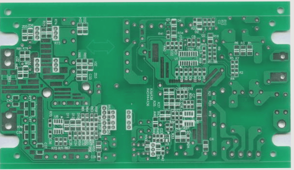
The basic process can be divided into three steps: PCB schematic design, netlist generation, and printed circuit board design. Specific requirements exist for both PCB component layout and trace routing.
For instance, minimize input and output wiring to reduce interference. Ensure separate routing for parallel signal lines with a ground wire in between, and aim for perpendicular alignment of adjacent layer traces to minimize parasitic coupling. Separate power and ground planes should ideally be placed perpendicular to each other across different layers.
Regarding trace widths, a wider ground trace can serve as a loop for digital circuit PCBs to establish a solid ground network (which is not suitable for analog circuits), utilizing large copper areas.
The following article elaborates on principles and key considerations in the PCB design of microcontroller control boards.

1. PCB Component Layout
When laying out components, ensure that related components are positioned as closely as possible. For instance, place the clock generator, crystal oscillator, and CPU clock input in proximity to minimize noise interference.
Components prone to noise, such as PCB current circuits and high-current switching circuits, should be segregated from logic control circuits and storage circuits (ROM, RAM). If feasible, isolate these circuits onto separate boards to enhance anti-interference measures and circuit reliability.
2. Decoupling Capacitors
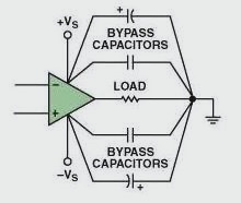
Install decoupling capacitors adjacent to critical components like ROM, RAM, and other chips. Circuit board traces, pin connections, and wiring can introduce significant inductance effects leading to switching noise spikes on the Vcc trace.
To mitigate these spikes, place a 0.1uF electronic decoupling capacitor between VCC and power ground. For surface mount components, directly mount chip capacitors to the Vcc pin of components.
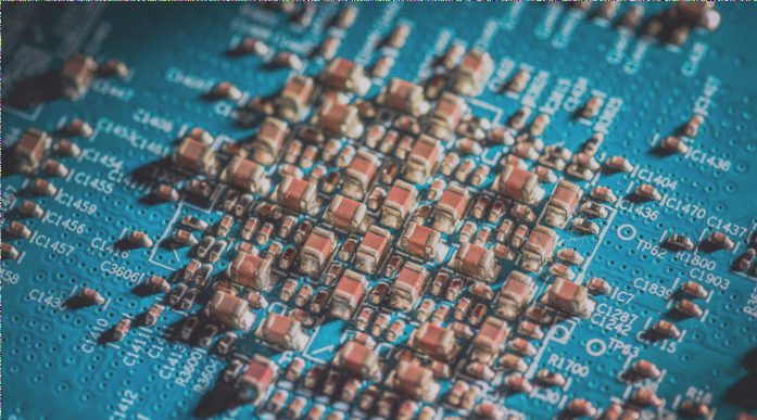
Prefer ceramic capacitors due to their lower electrostatic loss (ESL), high-frequency impedance, and stable dielectric properties over time and temperature. Avoid tantalum capacitors as they exhibit higher impedance at higher frequencies.
Consider the following when placing decoupling capacitors:
3. PCB Grounding Design
In single-chip microcomputer control systems on PCBs, various ground types exist, such as system ground, shield ground, logic ground, and analog ground. Proper grounding layout significantly impacts the circuit board’s immunity to interference.
When designing PCB grounding and grounding points, address the following considerations:
4. Miscellaneous
Besides power line layout, trace width should be maximized according to current requirements. Align power and ground line routing direction with data line routing in PCB layout. Additionally, utilize ground planes to cover unused areas on the circuit board bottom to enhance interference resistance.
Data line width should be sufficiently wide to minimize impedance, with a minimum width of 0.3mm (12 mils), ideally ranging from 0.46 to 0.5mm (18 mils to 20 mils).
Since each via on the circuit board adds approximately 10pF capacitance, which can interfere with high-frequency PCB circuits, minimize the number of vias in PCB layout. Excessive vias also compromise the mechanical integrity of the circuit board.
For instance, minimize input and output wiring to reduce interference. Ensure separate routing for parallel signal lines with a ground wire in between, and aim for perpendicular alignment of adjacent layer traces to minimize parasitic coupling. Separate power and ground planes should ideally be placed perpendicular to each other across different layers.
Regarding trace widths, a wider ground trace can serve as a loop for digital circuit PCBs to establish a solid ground network (which is not suitable for analog circuits), utilizing large copper areas.
The following article elaborates on principles and key considerations in the PCB design of microcontroller control boards.
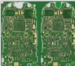
1. PCB Component Layout
When laying out components, ensure that related components are positioned as closely as possible. For instance, place the clock generator, crystal oscillator, and CPU clock input in proximity to minimize noise interference.
Components prone to noise, such as PCB current circuits and high-current switching circuits, should be segregated from logic control circuits and storage circuits (ROM, RAM). If feasible, isolate these circuits onto separate boards to enhance anti-interference measures and circuit reliability.
2. Decoupling Capacitors
Install decoupling capacitors adjacent to critical components like ROM, RAM, and other chips. Circuit board traces, pin connections, and wiring can introduce significant inductance effects leading to switching noise spikes on the Vcc trace.
To mitigate these spikes, place a 0.1uF electronic decoupling capacitor between VCC and power ground. For surface mount components, directly mount chip capacitors to the Vcc pin of components.
Prefer ceramic capacitors due to their lower electrostatic loss (ESL), high-frequency impedance, and stable dielectric properties over time and temperature. Avoid tantalum capacitors as they exhibit higher impedance at higher frequencies.
Consider the following when placing decoupling capacitors:
3. PCB Grounding Design
In single-chip microcomputer control systems on PCBs, various ground types exist, such as system ground, shield ground, logic ground, and analog ground. Proper grounding layout significantly impacts the circuit board’s immunity to interference.
When designing PCB grounding and grounding points, address the following considerations:
4. Miscellaneous
Besides power line layout, trace width should be maximized according to current requirements. Align power and ground line routing direction with data line routing in PCB layout. Additionally, utilize ground planes to cover unused areas on the circuit board bottom to enhance interference resistance.
Data line width should be sufficiently wide to minimize impedance, with a minimum width of 0.3mm (12 mils), ideally ranging from 0.46 to 0.5mm (18 mils to 20 mils).
Since each via on the circuit board adds approximately 10pF capacitance, which can interfere with high-frequency PCB circuits, minimize the number of vias in PCB layout. Excessive vias also compromise the mechanical integrity of the circuit board.

