PCB Design Best Practices for High-Performance Circuits
When it comes to PCB design, taking a hands-on approach can make all the difference. By personally handling component placement and routing, you can ensure that your design meets the highest standards of performance and reliability. Providing detailed explanations for your routing choices can also help your colleagues enhance their own design skills.
Recently, discussions in the msOS group have centered around PCB wiring, especially concerning stepper motors. Understanding PCB wiring is crucial for creating efficient paths that allow electrical signals to flow seamlessly between components.
Understanding PCB Wiring
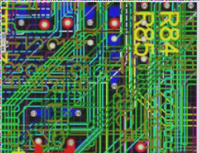
PCB wiring involves creating paths on a circuit board to connect components and facilitate the flow of electrical signals. Just like roads connect cities, PCB traces guide signals to their destinations, ensuring proper functionality.
Considerations for Different Circuits
In low-frequency circuits, simple loops are sufficient for signal paths. However, high-speed circuits, like those involving electromagnetic fields, require more complex transmission lines to manage impedance and behavior. For instance, differential signaling is vital for protocols such as USB and Ethernet.
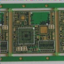
Utilizing Multilayer PCBs
For complex PCBs with many components, multilayer PCBs are essential. By using a multilayer design with a dedicated ground layer, you can reduce signal traces and maintain signal quality. The reference ground minimizes noise and electromagnetic interference, crucial for high-performance circuits.
Designing Ground Layers
When dealing with crossover signals on a double-sided PCB, keeping trace jumpers short is key to maintaining signal integrity. Long jumpers can disrupt the ground reference, leading to degraded signal quality. In such cases, opting for a multilayer PCB design can offer a more effective solution.
The Importance of Ground Layer in PCB Design
The ground layer in a PCB plays a crucial role in maintaining signal integrity by providing a stable reference point. It is essential to ensure that the reference ground remains undivided and uninterrupted to maximize its effectiveness.
Considerations for Signal Trace Spacing and High Frequencies
When routing signal traces, especially high-speed ones, it is important to maintain a proper distance between them. Just like trains on parallel tracks can experience interference due to proximity, closely spaced signal traces can also interfere with each other. This is particularly critical in high-frequency circuits where signal integrity is more vulnerable to interference.
Managing High-Current Circuits for Signal Integrity
In circuits with high-current or high-voltage components, such as power supply circuits, it is crucial to separate power and signal traces. High-current paths can introduce noise or impact nearby signal traces, leading to signal degradation. By keeping power and signal traces apart, interference can be minimized.
Guidelines for PCB Trace Layout Design
For standard PCB designs, it is recommended to place the reference ground approximately 1mm from the board’s edge, with signal traces also positioned about 1mm away from the reference ground. This layout creates a controlled environment within the PCB, confining signals and reducing electromagnetic emissions (EMC) for improved performance.
In essence, PCB design principles mirror road construction practices. Just as roads are meticulously planned to prevent traffic congestion and ensure smooth travel, PCB trace layout must be carefully executed to guarantee optimal signal integrity and minimal interference. By considering factors like ground layers, signal trace spacing, and trace routing, high-speed signals can be effectively managed, resulting in efficient PCB designs.