As the carrier of various components and the center of circuit signal transmission, the PCB board has become the most essential and critical element of electronic information products. The quality and reliability of PCBs directly influence the overall performance and dependability of the equipment. With the trend towards miniaturization of electronic products and the environmental demands for lead-free and halogen-free materials, PCBs are evolving towards higher density, higher Tg, and greater environmental compliance. However, due to cost constraints and technical challenges, numerous failure issues have arisen during the production and application of PCBs, leading to significant quality disputes. To identify the root causes of these failures, find solutions, and assign responsibilities, it is essential to conduct thorough failure analysis on the incidents that have occurred.
**Basic Procedure of Failure Analysis**
To accurately ascertain the cause or mechanism of PCB failures, it is crucial to follow established principles and analytical processes; otherwise, valuable information may be overlooked, hindering further analysis or leading to incorrect conclusions. The general procedure begins with identifying the failure phenomenon, followed by determining the failure location and mode through information gathering, functional testing, electrical performance testing, and basic visual inspection—this involves pinpointing the specific failure site. For simpler PCBs or PCBAs, identifying the failure location is relatively straightforward. However, for more complex devices such as BGA or MCM packages, defects may not be easily visible under a microscope, making identification more challenging. In such cases, additional methods may be required for accurate determination.
—
Let me know if you need any more changes!
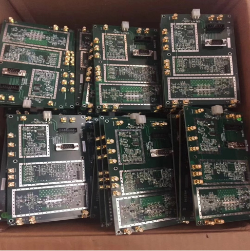
1. First, we must analyze the failure mechanism, meaning we employ various physical and chemical methods to investigate the causes behind PCB failures or defects, such as virtual welding, contamination, mechanical damage, moisture stress, medium corrosion, fatigue damage, CAF or ion migration, and stress overload.
2. Next comes the failure cause analysis, which involves understanding the failure mechanisms and processes to identify the root cause of the issues, conducting tests for verification when necessary. It is essential to perform thorough testing to accurately determine the cause of the induced failure, providing a focused basis for subsequent improvements.
3. Finally, based on the test data, facts, and conclusions gathered during the analysis, we compile a failure analysis report. This report must clearly present the facts, maintain strict logical reasoning, and be well-organized, avoiding any unfounded assumptions.
4. During the analysis, adhere to the basic principles that analytical methods should progress from simple to complex and from external to internal, ensuring samples remain intact for later use. This approach prevents the loss of critical information and avoids introducing new, man-made failure mechanisms.
5. This process resembles a traffic accident; if involved parties destroy evidence or flee the scene, it complicates accurate responsibility determination. Similarly, in PCB or PCBA failure analysis, if solder joints are repaired with a soldering iron or the PCB is forcibly cut, analysis becomes impossible as the failure site is compromised, particularly when there are few failed samples.
6. **Failure Analysis Technology**
**Optical Microscope**
The optical microscope is primarily utilized for inspecting the PCB’s appearance, identifying failure locations and associated physical evidence, and making initial judgments about the failure mode. Visual inspections focus on PCB contamination, corrosion, burst locations, circuit layout, and failure patterns, determining if issues are batch-related or localized.
7. **X-ray (X-ray)**
For components that are not visually accessible and to detect internal defects in PCB through-holes, an X-ray fluoroscopy system is employed. This system uses varying material thicknesses or densities to create images based on X-ray absorption principles, primarily checking internal defects in PCBA solder joints and positioning of defective solder joints in high-density packages like BGA or CSP.
8. **Slice Analysis**
Slicing analysis involves obtaining the cross-sectional structure of the PCB through sampling, embedding, slicing, polishing, etching, and observing. This method provides valuable microstructural information about the PCB’s quality (e.g., through holes, plating), forming a solid basis for future quality improvements. However, it is destructive, and the sample is irrevocably damaged once sectioned.
9. **Scanning Acoustic Microscope**
Currently, the C-mode ultrasonic scanning acoustic microscope is mainly applied in electronic packaging or assembly analysis. It images based on amplitude, phase, and polarity changes resulting from high-frequency ultrasonic waves reflecting off discontinuous material interfaces, scanning information along the Z-axis in the X-Y plane.
10. **Micro-infrared Analysis**
Micro-infrared analysis combines infrared spectroscopy with microscopy, leveraging different materials’ absorption characteristics. This method analyzes the compound composition of materials, and by aligning visible and infrared light paths, it enables the detection of trace organic pollutants within the visible field of view.
11. **Scanning Electron Microscope Analysis (SEM)**
The scanning electron microscope (SEM) is a powerful imaging system for failure analysis, commonly used for observing topography. Modern SEMs can magnify structures and surface features hundreds of thousands of times for detailed examination.
12. **Thermal Analysis**
**Differential Scanning Calorimeter (DSC)**
Differential Scanning Calorimetry measures the power differences between input materials and reference materials concerning temperature (or time) under controlled conditions. This analytical method explores the relationship between heat and temperature, allowing for the study of materials’ physical, chemical, and thermodynamic properties, particularly focusing on the curing degree and glass transition temperature of various polymers used on PCBs, which influence reliability.
13. **Thermomechanical Analyzer (TMA)**
Thermal Mechanical Analysis technology evaluates the deformation characteristics of solids, liquids, and gels under controlled thermal or mechanical forces. It helps investigate the correlation between heat and mechanical properties, with a focus on measuring linear expansion coefficients and glass transition temperatures, crucial for preventing metallized hole fractures during soldering and assembly.
14. **Thermogravimetric Analyzer (TGA)**
Thermogravimetric Analysis measures the relationship between a substance’s mass and temperature (or time) under programmed conditions. In PCB analysis, this method is primarily used to assess the thermal stability or decomposition temperature of PCB materials; low decomposition temperatures can lead to failures like delamination or explosions during high-temperature soldering processes.

