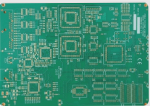
PCB Schematic Component Design: Detailed Process
1. Search for Existing Components
- Explore the PROTEL component library for the required component.
- If found, place the component in your schematic.
2. Creating a New Component if Not Available
- If the component is missing, create a new one in the Sch.lib library.
Process:
- Search for a similar component in the original library.
- Change the cursor to a cross cursor and select a reference point.
3. Create a New Device in the Sch.lib File
- Switch to the Sch.lib file.
- Create a new device using the “Create Component” shortcut.
- Rename the component to match the required one.
4. Paste the Existing Component into the New Library
- Access the “SCH Lib” tab at the bottom right.
- Right-click in an empty area, choose “Paste” to insert Component 1.
5. Modify the Pin Properties
- Adjust pin names, numbers, and functions to match requirements.
6. Perform Component Rule Check
- Run “Component Rule Check” to verify component parameters.
7. Final Steps
- After passing the check, the component is ready for use in your design.
By following these steps, you can efficiently manage PCB component design, ensuring accuracy and compliance with standards.
PCB Design Process: Effective Strategies
1. Schematic Design
In PCB design, start by creating a schematic file and loading necessary component libraries. Place components on the schematic sheet and wire connections according to design requirements.
For complex designs, consider a hierarchical schematic approach to simplify and organize the circuit.
2. Component Packaging Design
After schematics, focus on designing or modifying component PCB packages. Copy existing packages and make attribute adjustments to meet specifications.
Ensure correct alignment by setting the package reference point at the first pin. Run a Component Rule Check to validate the package against design rules.
3. PCB Layout Design

PCB Design Process: A Step-by-Step Guide
1. Setting Up the PCB Layout
After preparing the schematic and component packages, the next crucial step in PCB design is creating a new PCB file. Import the netlist to ensure all electrical connections are transferred from the schematic.
2. Defining PCB Size and Shape
Prior to layout and routing, it’s essential to define the PCB size and shape. Select the Keep-out Layer and draw the board outline using the Draw Line tool. This step helps establish the physical dimensions of your PCB, with the outline typically appearing in pink as part of the keep-out layer.
3. Component Placement and Optimization
Once the size and shape are set, utilize automatic component placement to arrange components on the PCB. While the software will attempt to optimize placements, manual adjustments may be necessary to enhance routing efficiency or meet specific design requirements.
4. Routing and Design Rule Checks
Proceed to route the PCB after component placement. Automatic routing tools can aid in this process, but manual routing may be needed for optimal performance and signal integrity. Regular Design Rule Checks (DRC) are crucial to ensure compliance with electrical and mechanical constraints, detecting issues like trace width violations or incorrect layer configurations.
General Workflow and Tips for PCB Design Success
- Schematic Design as the Foundation: Starting with a well-defined schematic is crucial, as it ensures correct electrical connections and understanding of circuit functionality.
- Hierarchical Design for Complex Circuits: Implement a hierarchical design approach for managing large designs and simplifying troubleshooting.
- Software Connectivity and Testing: Pay attention to software behavior to avoid hidden connectivity issues that might arise later without proper testing.
- Structured Workflow to Minimize Mistakes: Following a structured workflow from schematic design to PCB layout helps in creating a functional and manufacturable final design.
Conclusion
Adhering to a logical and systematic approach in PCB design leads to efficiency and accuracy. While shortcuts may seem appealing, especially in simpler designs, a structured process ensures higher quality and success in complex projects. Prioritize verifying electrical connectivity, optimizing component placement, and adhering to design rules to prevent costly errors in the long run.


