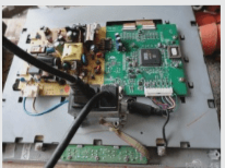
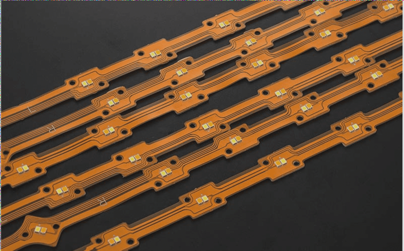
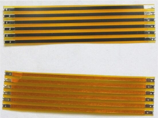
Lead-free PCBA processing refers to the manufacture of PCBA without the use of lead at any stage. Traditionally, lead has been integral to the PCB soldering process. However, due to its toxicity and harmful effects on humans, the EU Restriction of Hazardous Substances Directive (RoHS) prohibits lead in PCBA processing. Substituting lead with less toxic alternatives has minimal impact on the overall PCBA process. This article provides a detailed, step-by-step introduction to the lead-free PCBA process.
Lead-free PCBA Guide
The lead-free PCBA processing encompasses two primary components: the pre-assembly process and the active assembly process. The steps involved in lead-free PCBA are outlined below.
Pre-assembly Steps
Lead-free PCB manufacturing consists of three essential pre-assembly steps. These steps establish a solid foundation for precise and error-free PCB assembly. The pre-assembly steps for lead-free PCB assembly include the following.

**Analyze:**
1. **Analysis:**
Analysis is a process akin to prototyping. The manufacturer uses the completed lead-free PCB as the prototype. This may include a fully operational PCB, a defective one, or a dummy component. The template utilized for assembly is outlined by contour. The lead-free component design is compared with the prototype to ensure compatibility.
2. **Solder Paste Inspection:**
Since lead-free solder joints exhibit a metallic appearance that significantly differs from lead-based solders, meticulous inspection is crucial. The PCB shape and solder paste must be examined in accordance with the IPC-610D standard to confirm that the lead-free solder joints are robust and secure. Additionally, moisture content is assessed at this stage, as lead-free soldering is more susceptible to high moisture levels compared to traditional soldering.
3. **Bill of Materials (BOM) and Component Analysis:**
During this phase, the customer must verify the bill of materials (BOM) to confirm that all components are lead-free. Given that lead-free components are vulnerable to moisture, manufacturers should bake them in an oven. Once these preliminary steps are completed, the actual lead-free assembly process can commence.
4. **Active Assembly Steps:**
In the active assembly process, PCB assembly is conducted. The steps involved in active lead-free assembly are as follows.
5. **Template Placement and Solder Paste Application:**
In this step, the lead-free template for the forming stage is positioned on the board. Lead-free solder paste is then applied, typically using SAC305 as the solder paste material.
6. **Component Installation:**
After the solder paste application, components are installed onto the board. This placement can be performed manually or with automated machinery. It is a pick-and-place operation; however, the components used must be verified and marked during the BOM verification stage. The machine or operator selects the labeled components and positions them in the designated spots.
7. **Welding:**
Lead-free through-hole or manual soldering is executed at this stage. Regardless of the method used, whether THT or SMT, soldering must remain lead-free.
8. **Circuit Board Placement in the Reflow Oven:**
RoHS-compliant PCBs require high-temperature heating to uniformly melt the solder paste. Therefore, the PCBs are placed in a reflow oven where the solder paste is melted. The board is then cooled to room temperature to solidify the molten solder paste, helping to secure the components in place.
9. **Test and Packaging:**
The PCB has undergone testing in accordance with the IPC-600D standard. This stage involves testing the solder joints. Visual inspections are followed by Automated Optical Inspection (AOI) and X-ray inspection. Physical and functional tests are performed before packaging.
10. **Packaging of Lead-Free PCBs:**
For the packaging of lead-free PCBs, it is vital to use anti-static discharge bags. This is crucial to ensure that the final product is protected from static charges during transport.
11. **Conclusion:**
Despite having a comprehensive understanding of lead-free PCBA processing, further improvements can still be made by industry experts.
—
This version maintains the original meaning while enhancing clarity and flow.


