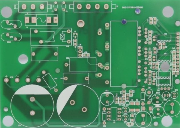
PCB Board Electroplating Process Overview:
- 1. Acid Bright Copper Electroplating
- 2. Nickel Electroplating / Gold Electroplating
- 3. Tin Plating
Process Flow:
- – Pickling
- – Full Plate Copper Plating
- – Pattern Transfer
- – Acid Degreasing
- – Secondary Countercurrent Rinsing
- – Micro-etching
- – Secondary Pickling
- – Tin Plating
- – Secondary Countercurrent Rinsing
- – Countercurrent Rinsing
- – Secondary Pickling
- – Pattern Copper Plating
- – Secondary Countercurrent Rinsing
- – Nickel Plating
- – Secondary Washing
- – Immersion in Citric Acid
- – Gold Plating
- – Recycling
- – 2-3 Grade Pure Water Washing
- – Drying
Latest Insights on the Process:
1. Pickling Process:
During pickling, oxides on the board surface are removed to activate it. It is crucial to maintain a short acid leaching time to prevent surface oxidation. The use of C.P grade sulfuric acid is recommended to ensure optimal results.
2. Full-board Copper Electroplating:
The process aims to protect the deposited copper and ensure uniform thickness distribution. Key parameters include maintaining specific copper sulfate and sulfuric acid content, adding chloride ions for gloss enhancement, and controlling the copper cylinder temperature.
Process maintenance involves replenishing copper gloss agent, regular pump checks, cleaning cathode rods, and weekly analysis of copper jar contents. Major treatment procedures include anode maintenance, tank liquid treatment, and activated carbon treatment for optimal results.
Anode copper balls containing phosphorus help reduce dissolution efficiency. Caution should be exercised when supplementing drugs like copper sulfate and sulfuric acid to prevent bath contamination.
Special Considerations for PCB Manufacturing Process
- Special attention is needed when adding chloride ions with low content (30-90ppm), as accurate measurement is crucial before addition.
- Calculation formula for drug addition:
- Copper sulfate (kg) = (75-X) × tank volume (liters) / 1000
- Sulfuric acid (liters) = (10%-X) g/L × tank volume (liters) or (liters) = (180-X) g/L × tank volume (liters)/1840
- Hydrochloric acid (ml) = (60-X) ppm × tank volume (liters)/385
Acid Degreasing Process
- Purpose and Function: Remove oxides and residual glue on the copper surface to ensure proper bonding force between copper and pattern electroplating copper or nickel.
- Reason for Acid Degreaser Usage: Graphic ink is sensitive to alkali, which could harm the graphic circuit.
- Control Parameters: Maintain degreaser concentration at around 10% and processing time at 6 minutes during production.
Micro-etching Procedure
- Purpose: Clean and roughen the copper surface to enhance bonding with patterned copper.
- Commonly Used Chemical: Sodium persulfate for stable and uniform roughening. Maintain a concentration of approximately 60 g/L with a processing time of about 20 seconds.
Pickling Process
- Function and Purpose: Remove oxides from the board surface and activate it. The typical concentration is 5%, with some at around 10%, mainly to prevent water contamination.
- Key Point: Keep acid leaching time short to avoid surface oxidation. Promptly replace the acid solution if it becomes turbid or if the copper content exceeds acceptable levels.
- Recommended Acid: Use C.P grade sulfuric acid.
Pattern Copper Plating (Secondary Copper)
- Purpose: Ensure that each line and hole copper reaches the required thickness to meet the rated current load. Follow the same procedures as full-board electroplating on a PCB board.