Usually, the term PCBA is frequently encountered in the SMT industry. Today, let’s delve into the related terminology and the PCBA production process.
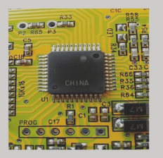
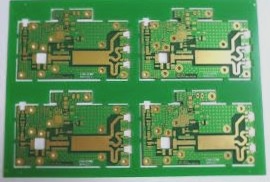
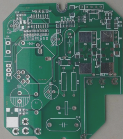
PCBA stands for Printed Circuit Board Assembly. Simply put, an empty PCB board undergoes SMT assembly and then completes the DIP plug-in process, resulting in what is known as PCBA. In layman’s terms, a PCB is a circuit board without components, while a PCBA is a circuit board with soldered electronic components.
The PCBA process integrates both SMT and DIP processes. Depending on different production requirements, it can be categorized into single-sided SMT placement, single-sided DIP insertion, single-sided mixed packaging, single-sided mixed placement and insertion, double-sided SMT placement, and double-sided mixed installation processes. The PCBA process includes steps such as carrier board preparation, printing, patching, reflow soldering, plug-in, wave soldering, testing, and quality inspection. Refer to the PCBA process flow chart below for further details.

**Brief Analysis of PCBA Production Process and Terminology Learning**
Different types of PCB boards involve various processes. Here is a brief overview of these processes:
1. **Single-Sided SMT Mounting**: Solder paste printing – component placement – reflow soldering. Solder paste is applied to the component pads; after printing on the bare PCB, electronic components are placed and then soldered through reflow soldering.
2. **Double-Sided SMT Mounting**: Solder paste printing on side A – component placement – reflow soldering – flipping – solder paste printing on side B – component placement – reflow soldering. To enhance aesthetics and functionality, some PCB designs use double-sided mounting, with IC components on side A and chip components on side B, optimizing PCB space.
3. **Single-Sided Mixed Assembly (SMD and THC on the Same Side)**: Solder paste printing – component placement – reflow soldering – manual through-hole component insertion (THC) – wave soldering.
4. **Single-Sided Mixed Assembly (SMD and THC on Both Sides)**: Red glue printing on side B – component placement – red glue curing – flipping – through-hole insertion on side A – wave soldering on side B.
5. **Double-Sided Mixed Assembly (THC and SMD on Both Sides of A, SMD on Both Sides of B)**: Solder paste printing on side A – component placement – reflow soldering – flipping – red glue printing on side B – component placement – red glue curing – flipping – through-hole insertion on side A – wave soldering on side B.
6. **Double-Sided Mixed Packaging (SMD and THC on Both Sides of A and B)**: Solder paste printing on side A – component placement – reflow soldering – flipping – red glue printing on side B – component placement – red glue curing – flipping – through-hole insertion on side A – wave soldering on side B – through-hole component placement on side B.
The following two methods are used for both sides: The first method involves PCBA assembly with three heating cycles, which is less efficient and has a lower pass rate due to the red glue process; it is not recommended. The second method is suitable for PCBs with numerous double-sided SMD components and few THT components, where manual soldering is advised. For a large number of THT components, wave soldering is preferred.
In the soldering process, minimizing variables related to machinery and equipment is crucial. To ensure accuracy, use independent electronic devices such as thermometers for temperature detection and electric meters for precise machine parameter calibration.
PCBA transforms a bare PCB into a functional electronic product. Quality issues at any stage of the process significantly impact the final product quality.
PCBA stands for Printed Circuit Board Assembly. Simply put, an empty PCB board undergoes SMT assembly and then completes the DIP plug-in process, resulting in what is known as PCBA. In layman’s terms, a PCB is a circuit board without components, while a PCBA is a circuit board with soldered electronic components.
The PCBA process integrates both SMT and DIP processes. Depending on different production requirements, it can be categorized into single-sided SMT placement, single-sided DIP insertion, single-sided mixed packaging, single-sided mixed placement and insertion, double-sided SMT placement, and double-sided mixed installation processes. The PCBA process includes steps such as carrier board preparation, printing, patching, reflow soldering, plug-in, wave soldering, testing, and quality inspection. Refer to the PCBA process flow chart below for further details.

**Brief Analysis of PCBA Production Process and Terminology Learning**
Different types of PCB boards involve various processes. Here is a brief overview of these processes:
1. **Single-Sided SMT Mounting**: Solder paste printing – component placement – reflow soldering. Solder paste is applied to the component pads; after printing on the bare PCB, electronic components are placed and then soldered through reflow soldering.
2. **Double-Sided SMT Mounting**: Solder paste printing on side A – component placement – reflow soldering – flipping – solder paste printing on side B – component placement – reflow soldering. To enhance aesthetics and functionality, some PCB designs use double-sided mounting, with IC components on side A and chip components on side B, optimizing PCB space.
3. **Single-Sided Mixed Assembly (SMD and THC on the Same Side)**: Solder paste printing – component placement – reflow soldering – manual through-hole component insertion (THC) – wave soldering.
4. **Single-Sided Mixed Assembly (SMD and THC on Both Sides)**: Red glue printing on side B – component placement – red glue curing – flipping – through-hole insertion on side A – wave soldering on side B.
5. **Double-Sided Mixed Assembly (THC and SMD on Both Sides of A, SMD on Both Sides of B)**: Solder paste printing on side A – component placement – reflow soldering – flipping – red glue printing on side B – component placement – red glue curing – flipping – through-hole insertion on side A – wave soldering on side B.
6. **Double-Sided Mixed Packaging (SMD and THC on Both Sides of A and B)**: Solder paste printing on side A – component placement – reflow soldering – flipping – red glue printing on side B – component placement – red glue curing – flipping – through-hole insertion on side A – wave soldering on side B – through-hole component placement on side B.
The following two methods are used for both sides: The first method involves PCBA assembly with three heating cycles, which is less efficient and has a lower pass rate due to the red glue process; it is not recommended. The second method is suitable for PCBs with numerous double-sided SMD components and few THT components, where manual soldering is advised. For a large number of THT components, wave soldering is preferred.
In the soldering process, minimizing variables related to machinery and equipment is crucial. To ensure accuracy, use independent electronic devices such as thermometers for temperature detection and electric meters for precise machine parameter calibration.
PCBA transforms a bare PCB into a functional electronic product. Quality issues at any stage of the process significantly impact the final product quality.


