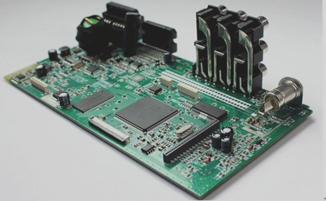
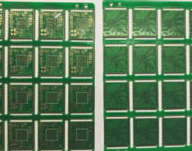
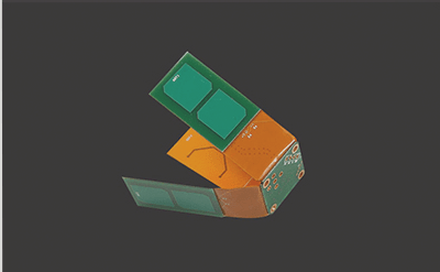
Electroless copper is a crucial step in the metallization of holes for PCBs and rigid-flex boards. Its primary objective is to create a very thin conductive copper layer on the walls of the holes and the copper surface, setting the stage for subsequent electroplating. Hole wall plating defects are common issues in PCB fabrication, particularly in the metallization of both flexible and rigid boards. These defects can lead to significant batch scrappage of printed circuit boards, making the resolution of plating issues a priority for PCB manufacturers. Effective control of this process is essential; however, due to the various factors that can lead to defects, it is vital to accurately assess the characteristics of these defects to devise effective solutions.
1. Hole wall plating cavities caused by PTH
The cavities in hole wall plating resulting from PTH are typically point-shaped or ring-shaped. The specific causes include:
(1) Bath temperature
The temperature of the bath significantly affects the activity of the solution. Each solution generally has specific temperature requirements, with some needing strict adherence. Therefore, constant monitoring of bath temperature is essential.
(2) Control of activation solution

Low concentrations of divalent tin ions can lead to the decomposition of colloidal palladium, negatively impacting palladium adsorption. However, if the activation solution is added consistently, significant issues can be avoided. A critical aspect of managing the activation solution is to prevent it from being stirred with air, as the oxygen can oxidize the divalent tin ions. Additionally, care must be taken to avoid water intrusion, which can result in the hydrolysis of SnCl₂.
(3) Cleaning Temperature
The cleaning temperature is often underestimated. The optimal temperature is above 20°C; temperatures below 15°C can adversely affect the cleaning results. In winter, water temperatures can drop significantly, particularly in northern regions. Low washing temperatures can cause the board’s temperature to remain low after cleaning. An immediate temperature increase upon entering the copper tank is crucial, as missing this “golden time” for copper deposition will impair the results. Therefore, in colder climates, monitoring the cleaning water temperature is essential.
(4) Use Temperature, Concentration, and Time of the Pore Modifier
The chemical solution’s temperature must be strictly controlled. Excessively high temperatures can lead to the decomposition of the pore modifier, reducing its concentration and compromising pore formation. A noticeable issue is the appearance of punctate voids in the glass fiber cloth within the holes. Achieving a suitable combination of temperature, concentration, and treatment time is vital for effective pore modification while also optimizing costs. Additionally, the concentration of copper ions in the solution must be carefully monitored.
(5) Use Temperature, Concentration, and Time of Reducing Agent
The reducing agent’s role is to eliminate residual potassium manganate and potassium permanganate after decontamination. Out-of-control parameters can adversely affect its effectiveness, resulting in visible punctate voids in the resin within the holes.
(6) Oscillator and Swing
Improper operation of the oscillator and swing can create ring-shaped cavities, primarily due to trapped bubbles in the holes. This issue is particularly pronounced in small orifice plates with high aspect ratios. Symmetrical cavities are a clear indicator, with normal copper thickness in the plated areas, where the secondary copper layer encapsulates the primary copper layer.
2. Hole Wall Plating Caused by Pattern Transfer
The hole wall plating issues arising from pattern transfer are mainly characterized by ring-shaped holes both at the orifice and within the holes. Specific causes include:
(1) Pre-Treatment Brush Plate
Excessive pressure from the brush plate can erode the copper layer on both the surface and PTH holes, preventing proper electroplating and resulting in ring-shaped voids. A clear indicator is the progressive thinning of the copper layer at the orifice, with the pattern plating layer encasing the entire board layer. Thus, controlling the brushing pressure through a wear scar test is necessary.
(2) Residual Glue at Orifice
Maintaining control over process parameters during pattern transfer is crucial. Inadequate pre-treatment drying, incorrect film temperature, and pressure can lead to residual glue at the orifice edge, forming annular cavities. This condition is identifiable by normal copper thickness in the hole but with a ring-shaped void at the entry, extending toward the pad, along with visible etching traces at the fault’s edge, where the pattern plating layer fails to cover the entire board.
(3) Pretreatment Micro-Etching
The micro-etching process during pre-treatment requires strict regulation, especially concerning the number of reworks on the dry film board. Insufficient electroplating uniformity may lead to excessively thin copper layers in the middle of the holes. Excessive reworking will cause the full-board copper layer to thin out, resulting in a ring-shaped copper-free area. This issue is marked by a gradual thinning of the plating layer throughout the hole, with the pattern plating layer enveloping the board’s plating layer.
3. Hole Wall Plating Caused by Pattern Plating
(1) Micro-Etching of Pattern Plating
Similar to pre-treatment micro-etching, the amount of micro-etching in pattern plating must be meticulously controlled. Defects can mirror those seen in dry-film pre-treatment micro-etching, with severe cases resulting in extensive copper-free areas along the hole wall, and a noticeably thinner surface copper layer. Regular measurements of the micro-etching rate are essential, and optimizing process parameters through DOE experiments is advisable.
(2) Poor Dispersion of Tin Plating (Lead Tin)
Factors such as inadequate solution performance or insufficient swing can lead to inadequate tin plating thickness. During subsequent film removal and alkaline etching, the tin and copper layers in the middle of the hole may be removed, forming ring-shaped voids. The telltale signs include normal copper thickness in the hole, evident etching traces at the fault’s edge, and incomplete coverage of the board by the pattern plating layer. To address this, incorporating tinning brighteners in the pickling step prior to tinning can enhance wettability and improve swing amplitude.
4. Conclusion
Numerous factors contribute to coating voids, with PTH coating voids being among the most common. By effectively controlling relevant PCB process parameters, the incidence of PTH coating voids can be significantly reduced. However, other contributing factors should not be overlooked. A thorough understanding of the causes and characteristics of coating voids is vital for timely and effective problem resolution, ensuring product quality is maintained.


