Functional Testing in PCBA Processing: Key Aspects to Consider
Functional Test Plan:
- DFM Instruction: Before SMT processing, follow a “design for testability” guide to ensure smooth testing throughout the design phase.
- Test Specification: Specify test requirements in the schematic, PCB layout, and microcontroller code for accuracy.
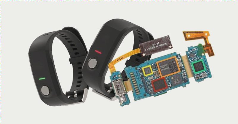
- Component Verification: Verify component voltage, touch sensor and LED installation, and microcontroller functionality.
Test Points:
- Easy Detection: Design PCB pads for easy detection without the need to probe individual component pins.
- Accessible Size: Ensure test points are of adequate size for easy contact with test probes.
In-system Programming:
- Structural Examination: Examine product structure to identify programming connectors or potential PCB positions.
- Programming Connector: Use an “in-system” programming connector for microcontroller installation and debugging during design.
- Cost Consideration: In mass production, in-system programming is often omitted to reduce costs.
Test Fixture:
- Prototype Testing: For early prototypes or small-scale designs, manual testing is a feasible option.
- Comprehensive Planning: Establish a test plan with checkboxes to ensure thorough testing and prevent critical step omissions.
Conclusion: Enhancing Functional Testing in PCBA Processing
Mastering the nuances of functional testing in PCBA processing involves meticulous planning, consideration of test points, in-system programming, and the use of test fixtures. By following a strategic approach, you can guarantee the quality and reliability of PCBA circuit board processing.