Efficiently Configuring Project Options for PCB Design Entry
Configuring project options for PCB design entry is crucial for guiding the design process effectively. Key parameters to set up include:
- Error Checking Parameters and Error Reporting: Establish criteria for identifying design issues early on to address them promptly.
- Connectivity Matrix: Defines electrical connections between components to ensure correct routing.
- Class Generator: Automatically organizes components into predefined classes for streamlined design.
- Comparator Setup: Enables comparison between design versions for efficient tracking of revisions.
- ECO Generation: Facilitates necessary changes during compilation without starting from scratch.
- Output Paths and Netlist Options: Set output locations for organized files.
- Multi-Channel Naming Formats: Define naming conventions for designs with multiple channels.
- Default Print Setups: Configure default printing settings for consistency.
- Search Paths: Specify directories for efficient workflow and file management.
- User-Defined Engineering Elements: Customize elements specific to your design workflow.
Applying Settings in Altium Designer
These settings are crucial for ensuring the design meets electrical integrity rules and is error-free. To configure project settings:
- Navigate to Project >> Project Options in the Project dialog box.
- Define parameters such as error checking, file comparison, and ECO generation.
- Customize output options via the File menu for assembly outputs and reports.
- Create a Job Options file through File >> New >> Output Job File for defining job options.
For detailed information on modifying error reporting settings, refer to Figure 6-9 below:

Utilizing Error Reporting in Altium Designer
Configure design checks by setting error severity levels for different types of errors:
- No Report
- Warning
- Error
- Fatal Error
Choose the appropriate level to flag critical issues, maintaining design integrity effectively.
Configuring the Connection Matrix
Utilize the connection data in the schematic diagram to identify and correct design issues efficiently. Altium Designer checks errors based on user-defined rules during project compilation, providing feedback for corrections.
The Importance of Connection Matrix in PCB Design
The Connection Matrix is a vital tool in PCB design, helping to define acceptable electrical connections and prevent errors. It visually illustrates the permissible connections between pins in the schematic, with options categorized as “Allow,” “Disallow,” “Warning,” or “Error.”
- Locate the Output Pin row and the Open Collector Pin column in the matrix.
- An orange square at their intersection indicates a connection triggering an error during compilation.
- Users can adjust error levels for specific connections based on project requirements.
Configuring the Comparator for Error-Free Designs
The Comparator interface is crucial for detecting changes between files during project compilation. When setting options, it’s essential to avoid selecting conflicting choices to ensure accurate comparisons.
- Navigate to the Associated with Component section.
- Set Changed Room Definitions and Extra Component Classes to Ignore Differences to prevent disruptions in the design process.
Compiling the Project for Validation
Compiling the project in Altium Designer is a critical step in identifying and resolving design issues. The Error Checking and Connection Matrix configurations are applied during compilation to validate the design.
- Select Project > Compile PCB Project to check for errors.
- Errors are displayed in the Messages panel, allowing for quick identification and correction.
Testing and Correcting Errors
To test error-checking, intentionally remove a connection and recompile the project. Detailed error information guides users to the exact location for correction.
- Undo the deletion to restore the connection and recompile the project.
- Use View > Fit All Objects to ensure proper alignment in the schematic.
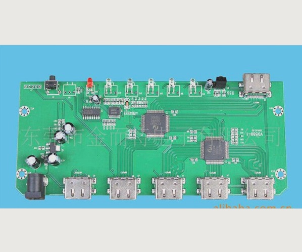
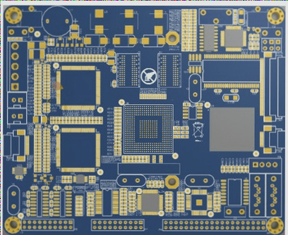
Transitioning to PCB Design
Once all errors are resolved, move forward to PCB layout design with confidence. Altium Designer’s tools facilitate error management, ensuring a reliable design ready for PCB layout.