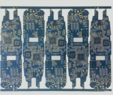
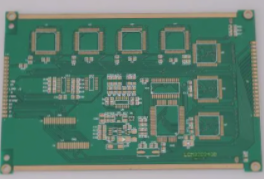
PCB Solder Mask and PCBA Manufacturing Optimization
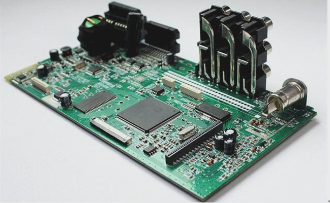
With the continuous advancements in electronic technology, the PCB assembly (PCBA) process is evolving to meet the demands for higher density and improved reliability. While manufacturing processes have improved, suboptimal solder pad and solder mask designs can complicate the surface-mount technology (SMT) soldering process, leading to quality issues in assembly.
Optimizing PCB Design for Better Manufacturability
When designing PCB layouts, it is crucial to adhere to industry standards like IPC-7351 and recommended pad sizes from device manufacturers. By adjusting pad sizes and solder mask dimensions based on these guidelines, engineers can enhance manufacturability and reduce the risk of soldering defects.
Addressing Unreasonable PCB Soldering Design Challenges
Unreasonable soldering design can lead to issues such as difficulties in solder paste application and component placement during PCBA manufacturing. Aligning pad and solder mask sizes with device specifications is crucial to ensuring product quality, yield, and reliability.
Enhancing PCB Engineering Design
Optimizing the solder mask process by covering solder pads and maintaining adequate mask bridges between pads is essential. When faced with suboptimal solder mask sizes, adopting a group pad window design process can help mitigate manufacturing challenges.
Meeting PCB Solder Mask Design Requirements
Research on PCB solder mask design and PCBA manufacturability is essential to address challenges in the manufacturing process. By following industry standards and optimizing solder mask and pad sizes, manufacturers can ensure the formation of proper solder mask bridges, enhancing isolation between pads.
Improving PCBA Process Capabilities
Continued research on PCB solder mask design and PCBA manufacturability is vital for enhancing process capabilities and ensuring the reliability of electronic devices.
The Importance of Solder Mask in PCB Design
The solder mask is crucial in preventing solder bridges that can lead to shorts during the assembly process. For high-density and fine-pitch pin PCBs, proper solder mask isolation is essential to ensure quality soldering.
Case Study: PCB Solder Mask Design
Extensive research on PCB solder mask design and its impact on PCBA manufacturability is essential for successful production.
Device Specifications:
- Pin center spacing: 0.65mm
- Pin width: 0.2–0.4mm
- Pin length: 0.3–0.5mm
Consequences of Poor PCB Soldering Design
Unreasonable PCB soldering design can significantly affect the PCBA manufacturing process, leading to potential quality risks.
PCB Layout Design Details:
- Solder pad size: 0.8mm x 0.5mm
- Solder mask size: 0.9mm x 0.6mm
- Center spacing of device pads: 0.65mm
- Edge spacing between solder pads: 0.15mm
- Solder mask spacing: 0.05mm
- Increased width of single-side solder mask by 0.05mm
Impact of Poor PCB Soldering Design
Failure to adhere to proper PCB soldering design can result in manufacturing delays and compromised soldering quality.
If you require PCB manufacturing services, feel free to contact us for assistance.