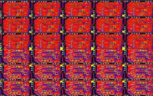
Copper cladding is a crucial aspect of PCB design. Essentially, it involves utilizing the unused space on a PCB as a reference plane and filling it with solid copper, a process commonly referred to as copper filling.
The significance of copper cladding lies in its ability to reduce ground impedance and enhance anti-interference capabilities, minimize voltage drop to improve power efficiency, and diminish loop area when connected to the ground wire. Most PCB manufacturers stipulate that PCB designers fill open areas of the PCB with copper sheeting or grid-like ground wires to maximize the PCB’s solder deformability.
At higher frequencies, the distributed capacitance of the wiring on a printed circuit board becomes significant. When the length exceeds 1/20 of the corresponding wavelength of the noise frequency, an antenna effect occurs, emitting noise outward through the wiring. Poorly grounded copper cladding can exacerbate this issue, turning the copper cladding into a conduit for spreading noise.
Hence, in high-frequency circuits, merely connecting the ground wire somewhere does not suffice; it must be grounded with a spacing of less than λ/20, with holes in the wiring, and a well-grounded floor plane in multilayer boards. When handled properly, copper cladding not only enhances current flow but also acts as a dual shield against interference.
There are two primary types of copper cladding: large area copper cladding and grid copper. It’s often debated whether large area or grid copper cladding is superior, but there’s no one-size-fits-all answer.
Large area copper cladding serves to increase current and shield, but it can cause warping or blistering during wave soldering. Therefore, large-area copper coating typically includes several grooves to mitigate copper foil foaming.
On the other hand, simple copper-clad grids primarily provide shielding, with reduced effectiveness in increasing current flow. From a heat dissipation perspective, grids are advantageous as they reduce the copper’s heating surface and offer some degree of electromagnetic shielding.
However, it’s crucial to note that grid lines run alternately, which can affect their efficacy depending on the circuit’s working frequency. When the electrical length matches the working frequency, the circuit’s functionality may be compromised, leading to signal interference. Therefore, when using grid copper cladding, it’s advisable to select based on the circuit board’s design requirements.
For high-frequency circuits with stringent interference demands, grid copper cladding is often preferred, while low-frequency circuits with high current requirements typically opt for complete copper cladding.
To achieve the desired effect of copper cladding, attention should be paid to grounding issues. In conclusion, properly managed copper cladding on a PCB is undoubtedly more beneficial than harmful. It reduces the backflow area of signal lines and mitigates external electromagnetic interference.