1. The purpose of this document is to outline the precautions for using PADS’s printed circuit board design software, PowerPCB, for printed circuit board design.

2. It also aims to provide design specifications for designers within a working group to enhance communication and facilitate mutual inspection among them.

3. Some errors may be disregarded; for instance, if part of the outline of certain connectors extends beyond the board frame, spacing errors may arise during checks.

4. Additionally, every time traces and vias are modified, the copper must be re-plated to ensure optimal performance.

2.6 Review

The review is based on the “PCB checklist,” which encompasses design rules, layer definitions, line widths, spacing, pad configurations, and via settings. It also emphasizes evaluating the rationality of the device layout, routing of power and ground networks, and high-speed clock networks. Additionally, it considers the wiring and shielding, placement and connection of decoupling capacitors, among other aspects. If the recheck is found unqualified, the designer must modify the layout and wiring. Once approved, both the rechecker and the designer must sign off separately.

2.7 Design output

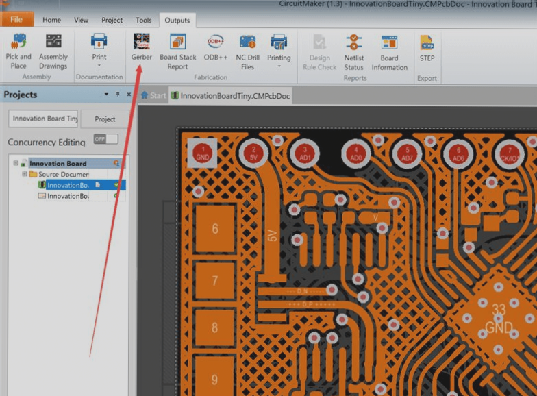
The PCB design can be exported to a printer or a Gerber file. The printer can output the PCB in layers, facilitating checks for designers and reviewers; the Gerber file is submitted to the board manufacturer for printed circuit board production. The output of the Gerber file is crucial, directly impacting the success of the design. The following points focus on important considerations when generating the Gerber file.

a. The layers to be output include wiring layers (top layer, bottom layer, and any middle wiring layers), power layers (VCC and GND layers), silk screen layers (top and bottom silk screens), solder mask layers (top and bottom solder masks), and drilling files (NCDrill).

b. If the power layer is set to Split/Mixed, select Routing in the Document section of the Add Document window. Each time the Gerber file is generated, use Pour Manager’s Plane Connect to pour copper on the PCB. If set to CAM Plane, select Plane and, in the Layer section, add Layer25, selecting Pads and Vias for this layer.

c. In the device setting window (press Device Setup), change the Aperture value to 199.

d. When setting the Layer for each section, select the Board Outline.

e. For the silk screen layer, do not select Part Type; instead, choose the top layer (or bottom layer) along with Outline, Text, and Line options of the silk screen layer.

f. When configuring the solder mask layer, select vias to indicate that no solder mask is applied to the vias; conversely, do not select vias if solder masks are to be applied, depending on the specific situation.

g. When generating drilling files, use the default settings of PowerPCB without any modifications.

h. After all Gerber files are output, open and print them using CAM350, and review them according to the “PCB Check List” by both the designer and the reviewer.


Let me know if you need any further adjustments!

Leave a Comment

Contact

WellCircuits
More than PCB

Upload your GerberFile(7z,rar,zip)