**Structure Level of Flexible Circuit Boards**
1. With the continuous development of PCB circuit boards, many types have emerged. Most can be classified into two categories: rigid and flexible circuit boards. Here, we will delve into the structure of flexible circuit boards.
2. Typically, PCB circuit boards are classified based on the number and thickness of conductive copper foils. They can be divided into single-layer boards, double-layer boards, multilayer boards, and double-sided boards. Each of these has distinct structures. Let’s delve into the details of these different features.
3. **Single-Layer Board Structure:** This is a relatively simple flexible board. Generally, it consists of base material, transparent glue, copper foil, and a protective film. The copper foil undergoes etching and other treatment processes to form the necessary circuits. The protective film requires drilling to expose the corresponding pads. After cleaning, the two layers are combined using a rolling method, and the exposed pads are electroplated with gold or tin for maintenance. Finally, the large board is stamped into smaller PCBs with the desired shape.

**Double-layer board structure:** When the circuit is too complicated for a single-layer board to handle routing or requires copper foil for grounding and shielding, a double-layer or multi-layer board becomes necessary.
**Structure of the multilayer board:** The primary distinction between a multilayer board and a single-layer board is the inclusion of via structures that connect each layer of copper foil. Typically, the initial process involves substrate + transparent glue + copper foil to create vias. Holes are drilled into the base material and copper foil, cleaned, and then plated with a specific thickness of copper to complete the vias. The subsequent production steps closely resemble those of a single-layer board.
**Double-sided board structure:** Double-sided boards have pads on both sides, primarily used for connecting with other PCBs. While the structure is similar to that of a single-layer board, the production process differs significantly. The raw materials include copper foil, protective film, and transparent glue. The process begins with drilling holes in the protective film according to the pad positions, followed by applying the copper foil. The pads and leads are then etched, and another protective film with pre-drilled holes is applied.
Although the structures of flexible circuit boards vary, many production processes share similarities, with specific adjustments made to accommodate different requirements.
**PCB circuit board electronic components layout restrictions:**
1. **Positioning hole:** Routing and component placement around positioning holes are prohibited, usually within a defined radius.
2. **Board edge:** No electronic components can extend beyond the PCB board (except for connectors). The distance from the board edge is influenced by the U-slot. Note that MLCC capacitors are sensitive to shear stress. Spacing requirements for traces, through holes, and test points from the board edge vary: traces require the smallest spacing, through holes are second, and test points require the largest spacing.
3. **Internal through holes:** Safety distances must be maintained around holes in the PCB board, though ground holes can be eliminated.
4. **Reference point:** Electronic components, copper traces, and solder masks must avoid proximity to reference points (fuzzy points). The recommended safety distance is 1.5 times the side length or diameter of the reference point.
5. **Antenna:** For RF receiving modules, ensure a safe distance around the antenna (PCB strip or metal).
6. **Height limit of electronic components:** The layout must account for potential recesses or ribs in the housing. Ensure that electronic components are placed at a distance from the housing to accommodate these features.
7. **Screw restrictions:** When using radiator fins or other screws, a safe distance must be maintained around the screws.
1. With the continuous development of PCB circuit boards, many types have emerged. Most can be classified into two categories: rigid and flexible circuit boards. Here, we will delve into the structure of flexible circuit boards.
2. Typically, PCB circuit boards are classified based on the number and thickness of conductive copper foils. They can be divided into single-layer boards, double-layer boards, multilayer boards, and double-sided boards. Each of these has distinct structures. Let’s delve into the details of these different features.
3. **Single-Layer Board Structure:** This is a relatively simple flexible board. Generally, it consists of base material, transparent glue, copper foil, and a protective film. The copper foil undergoes etching and other treatment processes to form the necessary circuits. The protective film requires drilling to expose the corresponding pads. After cleaning, the two layers are combined using a rolling method, and the exposed pads are electroplated with gold or tin for maintenance. Finally, the large board is stamped into smaller PCBs with the desired shape.
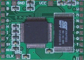
**Double-layer board structure:** When the circuit is too complicated for a single-layer board to handle routing or requires copper foil for grounding and shielding, a double-layer or multi-layer board becomes necessary.
**Structure of the multilayer board:** The primary distinction between a multilayer board and a single-layer board is the inclusion of via structures that connect each layer of copper foil. Typically, the initial process involves substrate + transparent glue + copper foil to create vias. Holes are drilled into the base material and copper foil, cleaned, and then plated with a specific thickness of copper to complete the vias. The subsequent production steps closely resemble those of a single-layer board.
**Double-sided board structure:** Double-sided boards have pads on both sides, primarily used for connecting with other PCBs. While the structure is similar to that of a single-layer board, the production process differs significantly. The raw materials include copper foil, protective film, and transparent glue. The process begins with drilling holes in the protective film according to the pad positions, followed by applying the copper foil. The pads and leads are then etched, and another protective film with pre-drilled holes is applied.
Although the structures of flexible circuit boards vary, many production processes share similarities, with specific adjustments made to accommodate different requirements.
**PCB circuit board electronic components layout restrictions:**
1. **Positioning hole:** Routing and component placement around positioning holes are prohibited, usually within a defined radius.
2. **Board edge:** No electronic components can extend beyond the PCB board (except for connectors). The distance from the board edge is influenced by the U-slot. Note that MLCC capacitors are sensitive to shear stress. Spacing requirements for traces, through holes, and test points from the board edge vary: traces require the smallest spacing, through holes are second, and test points require the largest spacing.
3. **Internal through holes:** Safety distances must be maintained around holes in the PCB board, though ground holes can be eliminated.
4. **Reference point:** Electronic components, copper traces, and solder masks must avoid proximity to reference points (fuzzy points). The recommended safety distance is 1.5 times the side length or diameter of the reference point.
5. **Antenna:** For RF receiving modules, ensure a safe distance around the antenna (PCB strip or metal).
6. **Height limit of electronic components:** The layout must account for potential recesses or ribs in the housing. Ensure that electronic components are placed at a distance from the housing to accommodate these features.
7. **Screw restrictions:** When using radiator fins or other screws, a safe distance must be maintained around the screws.

