Common methods for managing heat in PCBs include the use of heat sinks, thermal pads, thermal vias, copper pours, and thermal relief techniques. In PCB design, thermal management can be achieved by combining one or more of these methods. For example, a PCB design might incorporate heat sinks attached to high-power components, thermal vias to conduct heat, copper pours to distribute heat, and optimized component placement to improve airflow. In cases where surface area is limited, embedded copper structures can provide an effective solution for managing heat.
What is Embedded Copper Technology?
Embedded copper technology refers to the integration of solid copper into the layers of a PCB. Copper, due to its excellent thermal conductivity, serves as a heat sink, improving heat dissipation. This is particularly beneficial when placed underneath high-power components. Compared to other materials like aluminum or ceramics, which also have good thermal conductivity, copper offers a unique combination of exceptional thermal and electrical conductivity. Embedded copper is commonly used in industries such as power electronics, automotive, aerospace, and telecommunications, where effective heat management is essential.

Working Principle of Embedded Copper
The embedded copper coin, known for its superior heat conductivity, facilitates the efficient transfer of heat from components to the PCB. Acting as a thermal bridge, the copper coin quickly moves heat away from the component and into the PCB. Once inside the PCB, the heat is distributed across the surface, allowing for effective dissipation into the surrounding environment.
Types of Embedded Copper
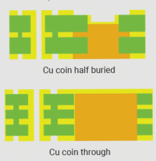
Buried copper coins are copper structures integrated into the inner layers of a printed circuit board. These coins have a thickness that is less than the overall thickness of the PCB. Embedded copper coins can be placed either on the surface or within the internal layers of the PCB. When positioned on the surface, the copper coins are visible, whereas they can also be strategically embedded within the layers of the PCB. In both configurations, these embedded copper coins create direct thermal pathways and electrical connections between different PCB layers, promoting efficient heat dissipation and electrical conductivity.
Potential Drawbacks
The use of embedded copper structures may increase the complexity of the PCB manufacturing process, reduce available space for routing traces and placing components, and raise production costs. As such, it is important to carefully evaluate the pros and cons when planning your PCB layout to determine if embedded copper is the best solution for your thermal management needs.
If you have any questions about PCBs or PCBA, please feel free to contact me at info@wellcircuits.com.

