Electroless Copper Plating Process for PCB Hole Metallization
Electroless copper plating, also known as sinking copper or PTH (Plated Through Hole), is a vital process in PCB manufacturing. It involves depositing copper onto PCB substrates without the need for an external electric current. This article delves into the stages of this process and provides insights based on industry expertise.
The Process Overview
The process begins with activating the PCB surface by applying an activator containing metal particles like palladium. These particles catalyze the copper deposition process. While palladium is commonly used, alternatives like colloidal copper are being explored to reduce costs.
Copper ions are then reduced on the palladium particles, forming copper crystal nuclei that facilitate further copper deposition. This self-sustaining process does not require external electrical input.
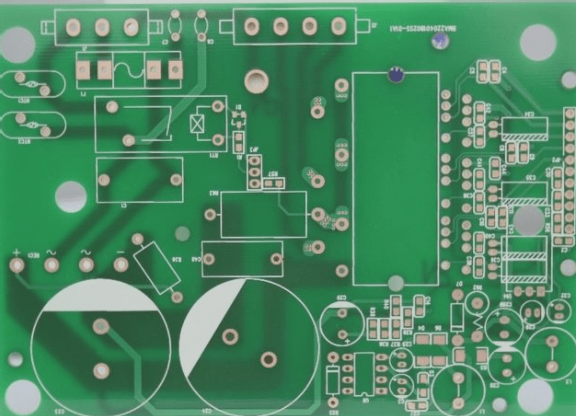
Electroless copper plating is crucial for PCB hole metallization, especially in multilayer PCBs where it ensures interlayer electrical connectivity.
PCB Hole Metallization Process Steps
- Drilling
- Deburring (Grinding the plate)
- Cleaning and Pre-treatment
- Micro-etching (Chemical roughening)
- Activation (Colloidal palladium treatment)
- Copper Plating (Sinking Copper)
- Washing and Drying
Pre-plating Treatment
Deburring
After drilling, burrs around hole edges can impact hole quality. Polishing the copper foil with water sandpaper or using mechanized deburring machines can effectively remove burrs. Advanced systems with rotating nylon brush rollers ensure thorough deburring.
Hole Cleaning Treatment
Cleaning holes is crucial to remove debris for proper adhesion. Modern practices involve using alkaline potassium permanganate solutions for effective cleaning.
Plating and Activation Treatments
Micro-etching (Chemical Roughening)
Chemical roughening of the PCB surface promotes better copper adhesion by creating a textured layer.
Activation (Colloidal Palladium Treatment)
Colloidal palladium treatment activates the surface for copper deposition. While palladium is effective, cost-efficient alternatives like colloidal copper are gaining popularity in the industry.
Copper Plating (Sinking Copper)
The copper plating process begins after activation, allowing for the deposition of copper onto the PCB substrate without the need for external electric current.
Metallization and Electroless Copper Plating Process for PCB Manufacturing
1. Hole Metallization and Surface Preparation
During hole metallization, copper ions are reduced on the palladium particles, forming a metallic layer inside the drilled holes. Thorough cleaning of the substrate before electroless copper plating is crucial to ensure strong bonding.
2. Copper Foil Roughening Treatment
The copper foil surface undergoes a chemical micro-etching process to create a micro-roughened, active copper surface that enhances bonding strength. Modern methods like sulfuric acid/hydrogen peroxide mixtures offer a more consistent etching speed and uniform roughening effect.
3. Activation
Activation involves coating the substrate surface with catalytic metal particles to facilitate smooth electroless copper plating. Common methods include sensitization-activation and colloidal solution activation.
4. Electroless Copper Plating
a. Plating Solutions
- Formula 1: Uses potassium sodium tartrate as the complexing agent. While easy to use, it has poor stability and can produce brittle copper plating.
- Formula 2: Utilizes EDTA-2Na for a higher operating temperature and improved stability, albeit at a higher cost.
- Formula 3: Incorporates a dual complexing agent, balancing performance between Formulas 1 and 2.
b. Stability of Electroless Copper Plating Solution
Formaldehyde disproportionation under alkaline conditions leads to solution instability, accelerating aging and depleting formaldehyde. Proper control of plating time is essential to prevent excessive plating layers that could weaken adhesion.
Final Treatment and Inspection
After copper plating, the PCB undergoes washing, drying, pickling, rinsing, and drying again to meet quality standards.
Conclusion and Industry Best Practices
Electroless copper plating is crucial in PCB manufacturing, requiring attention to detail at each step. Industry best practices like advanced deburring systems and optimized chemical treatments enhance product quality and reduce costs.
By monitoring and refining each stage of the process, PCB manufacturers ensure product reliability and performance while managing production costs effectively.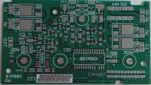
Copper Ions Disproportionation
In alkaline plating solutions, formaldehyde reduces Cu²⁺ to Cu⁺, leading to the formation of Cu₂O. This compound can further decompose into fine copper particles through disproportionation. These particles act as catalysts, speeding up the decomposition of the plating solution and making it unstable.
Improving Solution Stability
To tackle the instability of electroless copper plating solutions, several strategies can be implemented:
- Stabilizer Addition: Adding stabilizers like sulfur or nitrogen-containing compounds (e.g., bipyridine, potassium ferrocyanide, thiourea) can prevent the disproportionation of Cu⁺ ions, thus stabilizing the solution.
- Air Stirring: Introducing air into the solution can reduce the formation of Cu₂O, aiding in stabilizing the solution.
- Continuous Filtration: Regular filtration using a 5 µm filter can eliminate active particulate matter, preventing contamination of the solution.
- Polymer Compounds: Utilizing polymers with hydroxyl or ether groups (e.g., polyethylene glycol) can mask the copper particles formed during disproportionation, averting their catalytic effect on the solution breakdown.
- Workload Control: Monitoring and maintaining the workload below 1 dm²/L during continuous electroless copper plating can prevent overloading of the solution, which might cause premature decomposition.
Improving Toughness of the Electroless Copper Layer
For reliable PCB hole connections, the electroless copper layer must possess sufficient toughness. Inadequate toughness often stems from the release of hydrogen during the reduction of Cu²⁺ by formaldehyde. Although hydrogen does not co-deposit with copper, it can adsorb on the copper surface, forming bubbles that accumulate in the layer. These bubbles create voids, elevating the layer’s resistance and diminishing its toughness.
To enhance the toughness of the copper layer, hydrogen barrier agents are introduced into the plating solution. These agents hinder the buildup of hydrogen on the copper surface, ensuring a more uniform and sturdy copper layer.
By following these steps and implementing appropriate controls, PCB manufacturers can guarantee top-notch metallization and electroless copper plating, resulting in dependable and long-lasting PCB products.