PCB layout is a critical challenge that every PCB design engineer must address at the outset. This task involves making strategic decisions based on the components specified in the schematic and ensuring that certain devices are logically grouped together. One important consideration is the placement of temperature-sensitive components, such as sensors, which should be located away from heat-generating components like power converters. These temperature-sensitive devices can be adversely affected by thermal interference, leading to potential reliability issues.
For designs with multiple power rails, such as 12V and 15V power converters, it’s crucial to place them in different areas of the PCB. This separation helps mitigate the heat and electronic noise they produce, which can negatively affect the performance and reliability of surrounding components. Moreover, the positioning of power converters can influence the overall electromagnetic performance of the PCB, a key factor not only for functional performance but also for energy efficiency.
The electromagnetic characteristics of the PCB design also impact its compliance with regulatory standards, such as the CE mark required for products sold in Europe. This certification ensures that the PCB does not emit harmful interference to other systems. However, the issue of electromagnetic interference (EMI) is not limited to power supply components alone. Devices such as DC-DC converters and high-speed data converters are significant noise sources. If the PCB layout is not optimized, these devices can unintentionally radiate noise through the PCB traces, acting like antennas. This can lead to spurious emissions and abnormal frequency behavior, further compromising the performance and reliability of the system.
In summary, effective PCB layout is not just about fitting components onto the board but also involves strategic placement to manage heat dissipation, minimize electromagnetic interference, and meet regulatory requirements. Design engineers must carefully consider the interactions between components to ensure optimal performance, reliability, and compliance.

**Electromagnetic Interference (EMI) in PCB Design: Key Considerations and Solutions**
Far-field electromagnetic interference (EMI) can be mitigated by installing filters at noise points or using metal enclosures to shield the signals. However, one often overlooked factor in PCB design is the potential for the PCB itself to emit EMI. Proper attention to this aspect can enable the use of a more cost-effective housing for the equipment, which in turn helps reduce the overall system cost.
In PCB design, EMI is a critical issue that cannot be ignored. Electromagnetic crosstalk between signal lines can cause unwanted noise, disrupting signals and degrading the overall performance of the PCB. If this crosstalk is excessive, the signal may be entirely masked by the noise, requiring the use of an expensive signal amplifier to restore the signal integrity. By considering EMI in the early stages of PCB design, these issues can be avoided, saving both cost and design complexity.
The design of a PCB will vary depending on several factors, including the type of equipment, its intended usage, heat dissipation requirements, and the level of EMI exposure. A comprehensive design template can help standardize the process and ensure that all these variables are addressed efficiently.
Capacitance is another important consideration in PCB design. It impacts signal propagation speed and increases power consumption. Unintended capacitive effects can arise when adjacent signal lines or circuit layers couple with each other, forming parasitic capacitors. To reduce these effects, designers can take steps such as minimizing the length of parallel traces or introducing bends in the layout to break the coupling. However, these solutions must be balanced with the practical constraints of manufacturability, avoiding excessive bending that might lead to noise radiation or potential reliability issues.
Moreover, the spacing between signal traces must be carefully controlled. If traces are too close, they may create short loops, particularly at bends, leading to issues like metal “whiskers” or increased risk of cross-talk. Design rule checks can help identify areas where the risk of unwanted coupling is higher than usual.
This issue is particularly critical when designing the ground plane. A metal ground layer can block noise effectively, but it also introduces parasitic capacitance, which affects signal integrity and increases power consumption. Designers must strike a balance between effective noise shielding and minimizing the performance penalties introduced by the ground plane.
In multi-layer PCB designs, the through-hole design is one of the most controversial aspects. Through-holes that connect different layers of the PCB can negatively impact signal performance and reduce the overall reliability of the board. These through-holes introduce challenges in manufacturing and can lead to degraded signal integrity. Therefore, careful consideration of through-hole placement and routing is essential to maintain signal performance and improve the overall reliability of the PCB.
In conclusion, a well-thought-out PCB design that takes EMI, capacitance, trace spacing, and through-hole considerations into account can significantly improve the performance and reliability of the final product. Balancing these factors with manufacturability and cost-effectiveness is key to creating an optimal PCB design.
For designs with multiple power rails, such as 12V and 15V power converters, it’s crucial to place them in different areas of the PCB. This separation helps mitigate the heat and electronic noise they produce, which can negatively affect the performance and reliability of surrounding components. Moreover, the positioning of power converters can influence the overall electromagnetic performance of the PCB, a key factor not only for functional performance but also for energy efficiency.
The electromagnetic characteristics of the PCB design also impact its compliance with regulatory standards, such as the CE mark required for products sold in Europe. This certification ensures that the PCB does not emit harmful interference to other systems. However, the issue of electromagnetic interference (EMI) is not limited to power supply components alone. Devices such as DC-DC converters and high-speed data converters are significant noise sources. If the PCB layout is not optimized, these devices can unintentionally radiate noise through the PCB traces, acting like antennas. This can lead to spurious emissions and abnormal frequency behavior, further compromising the performance and reliability of the system.
In summary, effective PCB layout is not just about fitting components onto the board but also involves strategic placement to manage heat dissipation, minimize electromagnetic interference, and meet regulatory requirements. Design engineers must carefully consider the interactions between components to ensure optimal performance, reliability, and compliance.
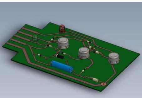
**Electromagnetic Interference (EMI) in PCB Design: Key Considerations and Solutions**
Far-field electromagnetic interference (EMI) can be mitigated by installing filters at noise points or using metal enclosures to shield the signals. However, one often overlooked factor in PCB design is the potential for the PCB itself to emit EMI. Proper attention to this aspect can enable the use of a more cost-effective housing for the equipment, which in turn helps reduce the overall system cost.
In PCB design, EMI is a critical issue that cannot be ignored. Electromagnetic crosstalk between signal lines can cause unwanted noise, disrupting signals and degrading the overall performance of the PCB. If this crosstalk is excessive, the signal may be entirely masked by the noise, requiring the use of an expensive signal amplifier to restore the signal integrity. By considering EMI in the early stages of PCB design, these issues can be avoided, saving both cost and design complexity.
The design of a PCB will vary depending on several factors, including the type of equipment, its intended usage, heat dissipation requirements, and the level of EMI exposure. A comprehensive design template can help standardize the process and ensure that all these variables are addressed efficiently.
Capacitance is another important consideration in PCB design. It impacts signal propagation speed and increases power consumption. Unintended capacitive effects can arise when adjacent signal lines or circuit layers couple with each other, forming parasitic capacitors. To reduce these effects, designers can take steps such as minimizing the length of parallel traces or introducing bends in the layout to break the coupling. However, these solutions must be balanced with the practical constraints of manufacturability, avoiding excessive bending that might lead to noise radiation or potential reliability issues.
Moreover, the spacing between signal traces must be carefully controlled. If traces are too close, they may create short loops, particularly at bends, leading to issues like metal “whiskers” or increased risk of cross-talk. Design rule checks can help identify areas where the risk of unwanted coupling is higher than usual.
This issue is particularly critical when designing the ground plane. A metal ground layer can block noise effectively, but it also introduces parasitic capacitance, which affects signal integrity and increases power consumption. Designers must strike a balance between effective noise shielding and minimizing the performance penalties introduced by the ground plane.
In multi-layer PCB designs, the through-hole design is one of the most controversial aspects. Through-holes that connect different layers of the PCB can negatively impact signal performance and reduce the overall reliability of the board. These through-holes introduce challenges in manufacturing and can lead to degraded signal integrity. Therefore, careful consideration of through-hole placement and routing is essential to maintain signal performance and improve the overall reliability of the PCB.
In conclusion, a well-thought-out PCB design that takes EMI, capacitance, trace spacing, and through-hole considerations into account can significantly improve the performance and reliability of the final product. Balancing these factors with manufacturability and cost-effectiveness is key to creating an optimal PCB design.

