Printed Circuit Board (PCB) Technology Overview
PCB, short for Printed Circuit Board, is a vital electronic component that provides support to electronic parts and establishes electrical connections between them. The term “printed” comes from the electronic printing process used during production.
Evolution of PCB Technology
In 1936, Austrian inventor Paul Eisler pioneered the concept of the printed circuit board, initially used in a radio device. By 1943, the United States began widespread military application, leading to official commercial recognition in 1948. Since the mid-1950s, PCB technology has seen extensive adoption.
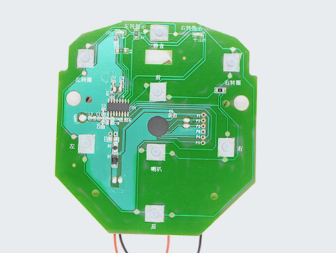
Types of PCB Circuit Boards
- Single-sided boards
- Double-sided boards
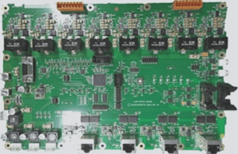
- Multi-layer boards
Materials and Cost Factors
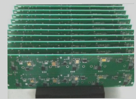
- PCBs categorized into soft and hard types
- Main material: copper-clad laminate for component support and electrical connections
- Cost influenced by material selection and production processes
Factors Affecting PCB Pricing
- Material choices and thickness variations
- Different production processes
- Complexity of PCB design
- Customer requirements and production efficiency
- Varied manufacturers and technical expertise
- Diverse payment methods and geographical pricing differences
Process Cost Considerations
The cost of PCB production depends on circuit density; lower wire density incurs separate pricing considerations.
Factors Affecting PCB Manufacturing Costs
- The presence of BGA on the board can lead to increased costs, with pricing varying based on specific locations.
- Surface treatment processes, such as lead tin spraying, OSP, and finishes like tin, silver, or gold, impact prices due to different technologies.
- Process standards, like IPC2 or higher standards for specific customer requirements, influence pricing, with IPC3, enterprise, or military standards potentially raising costs.
- Customized PCBs require meticulous cost calculations, considering material utilization and automated layout computations on standard-sized copper-clad laminates.
- PCB cost calculations are intricate, considering material, labor, and manufacturing costs from cutting to final quality control, with unique methods needed for specialized products like blind buried vias and immersion gold boards.
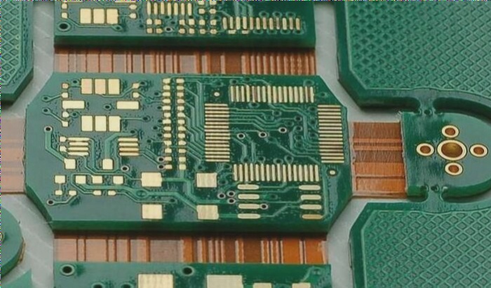
PCB Design and Wiring Rule Inspections
- Check spacing between lines, line to component pad, line to through hole, component pad to through hole, and between through holes to meet production standards.
- Verify appropriate widths of power and ground lines for low wave impedance and ensure proper ground line widening.
- Implement optimal measures for key signal lines, minimize lengths, and separate input and output lines from protection lines.
- Use separate ground wires for analog and digital circuits.
- Modify line shapes to prevent signal short circuits from added graphics and annotations.
- Ensure no process lines on the PCB, meet solder mask production requirements, and prevent interference of logos with device pads.
- Maintain the outer frame edge of the power ground layer in multi-layer PCBs to prevent exposure of copper foil and potential short circuits.
If you require PCB manufacturing services, feel free to contact us.