What specific aspects of the process are you most interested in exploring?
—
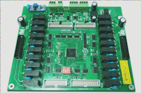
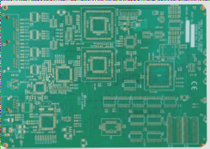
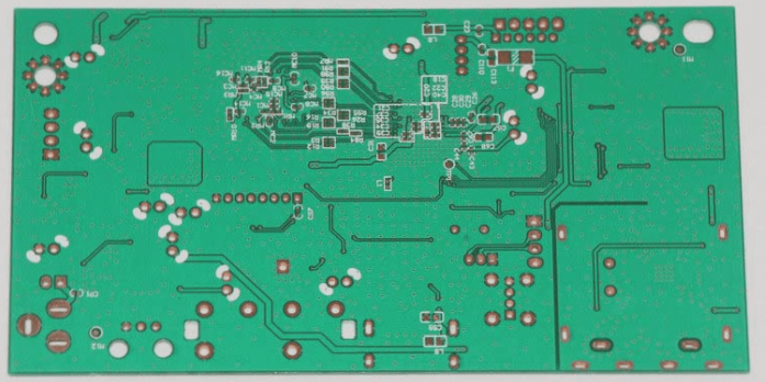
What is the process from bare PCB to PCBA? Let’s explain in detail below:
1. SMT Placement Process
SMT (Surface Mount Technology) is a widely used technique in the electronics assembly industry. In simple terms, it involves mounting surface-mounted components, which have either no leads or very short leads (referred to as SMC/SMD, or chip components in Chinese), directly onto the surface of a Printed Circuit Board (PCB) or other substrates. This process utilizes circuit assembly techniques like reflow soldering or dip soldering for soldering and assembly.
So, what preparations need to be made before SMT placement?
1. A MARK point must be present on the PCB, also known as a reference point, to facilitate accurate placement by the placement machine, serving as a point of reference.
2. A stencil should be created to assist in the deposition of solder paste, ensuring the precise amount of solder paste is applied to the correct positions on the empty PCB.
3. SMD Programming: According to the provided BOM list, components are accurately positioned and placed on the PCB through programming. Once all preparations are complete, the SMT process can commence.
First, the placement machine checks the orientation of the board using the MARK point sent in. Next, solder paste is applied to the stencil, allowing it to be deposited onto the PCB pads.
Following this, the placement machine places the components on the designated spots on the PCB according to the programming instructions. This is followed by reflow soldering, which effectively connects the components, solder paste, and the circuit board.
Finally, an automatic optical inspection is performed to verify the components on the PCB, assessing factors such as soldering quality, connection integrity, and device orientation. However, functional testing cannot be conducted at this stage due to un-soldered through-hole components.
It is important to note that some components have polarity or pin configurations, necessitating careful inspection of incoming materials to avoid placement errors, particularly with BGA packaged devices. Incorrect orientation can lead to time-consuming and labor-intensive disassembly and repair.
Next, the DIP Plug-In Process:
DIP (Dual In-Line Package) refers to devices that can be inserted and soldered onto the PCB, commonly known as plug-in components.
What preparations are necessary before the DIP plug-in?
1. Prepare the fixture and secure the PCB for easy transmission on the conveyor belt.
2. Adjust the pins of plug-in devices that are too long to the correct length.
3. Human intervention is required to insert the plug-in components into the corresponding via holes on the PCB.
The DIP plug-in process is generally simpler than the SMT process, requiring manual insertion of components into the holes, followed by passing through the wave soldering machine, where the plug-in devices are securely soldered to the PCB.
Some may worry about solder splashing across the board. The answer is no; solder in the solder pool adheres only where it contacts metal and does not bond with the green solder mask. This is the primary function of the solder mask.
After the plug-in devices are soldered, is the PCBA complete? Not quite, as the board must undergo further checks and functional verification after both the SMT and DIP processes.
3. Conducting Functional Testing on the Produced PCBA:
The functional testing of the produced PCBA consists of two steps:
Step 1: A visual inspection of the PCBA is performed to identify obvious defects, such as solder issues or missing components. Defective boards are sent for repair, while those without visible issues proceed to the next step.
Step 2: The PCBA is tested using a test fixture, which conducts a power-on functional test. This involves checking various test points on the PCBA, such as power cycles, relay activation, and communication checks, to confirm that each module operates correctly.
Through these two steps, not only can defective boards be identified, but potential issues can also be diagnosed, thereby streamlining subsequent repair efforts.
Thus, it is evident that throughout the transition from PCB bare board to PCBA, technicians implement rigorous and thorough testing at every stage to ensure the integrity of the production process. Only by maintaining these standards can we advance to the next step.
4. Waterproof, Dustproof, and Anti-Corrosion Treatment for PCBA:
The waterproof, dustproof, and anti-corrosion treatment involves spraying or dipping wax on the PCBA. Different companies may employ various methods: some manually apply conformal coating, others use machines for spraying, while some opt for dipping wax, and a few may forgo this treatment altogether.