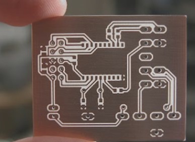
Understanding the Importance of PCB Ground Plane in Electronics
A PCB ground plane is a crucial element in electronic devices, aiding in noise reduction, signal recovery, and interference mitigation. Let’s delve into the significance of the PCB ground plane and its applications.
What is a PCB Ground Plane?
The PCB ground plane is a large metal area on a printed circuit board that serves as a common ground or energy supply potential. It helps in voltage return, signal recovery, and minimizing noise and interference between signals.
Key Roles of PCB Ground Plane:
- Voltage Recovery: Ensures reliable connections for power nets on the board.
- Signal Recovery: Facilitates smooth signal return, especially in multi-layered designs.
- Noise Reduction: Manages energy fluctuations to minimize noise during circuit operation.
Creating an Effective PCB Ground Plane:
Proper grounding is essential to avoid signal crosstalk, ground loops, and interference. Here are some key steps to follow:
- Validate Schematic Nets: Define ground or power plane nets correctly in the schematic.
- Utilize Internal Planes: Internal planes are crucial for creating an efficient ground plane.
- Polygon Pour: Consider using a polygon pour for a positive ground plane.
By adhering to these guidelines and utilizing CAD tools effectively, you can ensure a well-implemented PCB ground plane, leading to improved device performance and reduced signal issues.
Understanding the Importance of PCB Ground Plane
Having a solid understanding of the PCB ground plane is crucial for ensuring the proper functioning of your electronic devices. The ground plane serves as a reference point for all electrical signals on the board, providing stability and reducing electromagnetic interference.
Applications of PCB Ground Plane
- Signal Integrity: The ground plane helps maintain signal integrity by providing a stable return path for signals.
- EMI Reduction: By acting as a shield, the ground plane reduces electromagnetic interference, improving the overall performance of the circuit.
- Heat Dissipation: In high-power applications, the ground plane can help dissipate heat, preventing overheating of components.
Latest Developments in PCB Ground Plane Design
Recent advancements in PCB technology have led to the development of more efficient ground plane designs. Techniques such as split planes, stitching vias, and controlled impedance routing have enhanced the performance and reliability of PCBs.
Consulting Professionals for PCB Design
When in doubt about your PCB ground plane design, it is always advisable to seek guidance from experienced professionals in the field. Conducting thorough research and consulting with experts can help you make informed decisions and avoid costly mistakes.

