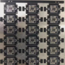
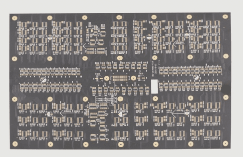
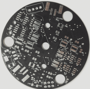
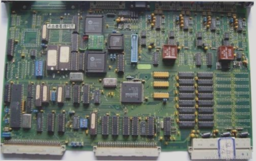
PCB Proofing Process Steps
-
Provide Necessary Documents
Submit process specifications and quantities to the manufacturer. For example, with Shenzhen Zhongqicheng PCB Factory, register on their platform, use code “R” to get a quotation, place an order, and track progress.
-
Cutting
Purpose: Segment large sheets into smaller panels meeting engineering data specifications.
Process: Large sheet → cutting according to MI specifications → curium board → beer fillet/grinding → panels ready.
-
Drilling
Purpose: Drill required apertures at designated locations adhering to specified dimensions.
Process: Stacked board pin → drilling → inspection/repair.
-
Immersion Copper
Purpose: Deposit a thin copper layer onto insulating hole walls.
Process: Rough grinding → hanging board → automatic copper sinking line → dipping in dilute H2SO4 → copper thickening.
-
Graphics Transfer
Transfer the image from production film to the board using the blue oil process or dry film process.
Additional PCB Proofing Steps
-
Graphic Plating
Purpose: Apply copper and gold-nickel or tin layers to the circuit pattern.
Process: Degrease → micro-etch → copper plate → tin plate.
-
Removal of the Film
Purpose: Strip anti-electroplating coating film with NaOH solution.
Process: Water film: soak in alkali → rinse → scrub; Dry film: pass through machine.
-
Etching
Purpose: Remove copper from non-circuit areas using a chemical reaction.
-
Green Oil
Purpose: Transfer graphics to protect the circuit during component welding.
Process: Print green oil → cure → expose → print both sides.
-
Characters
Purpose: Serve as identification markers.
Process: Print characters after green oil application.
-
Gold-Plated Fingers
Purpose: Enhance hardness and wear resistance with nickel/gold layers.
Process: Degrease → micro-etch → copper plate → nickel plate → gold plate.
-
Tin Plate (Parallel Process)
Purpose: Apply lead-tin layer for soldering performance.
Process: Micro-erosion → apply rosin → coat with solder → air cool.
-
Forming
Purpose: Shape boards through die stamping or CNC machining.
Note: CNC offers high accuracy, beer boards offer precision, hand forming is less accurate, and hand-cut boards are for simple shapes.
-
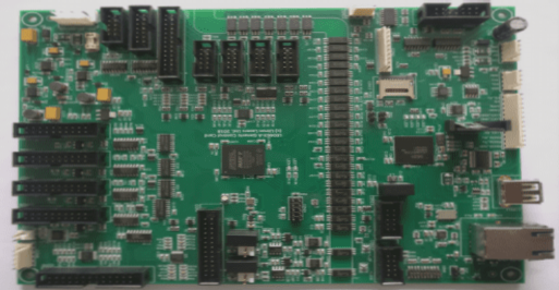
Testing
Purpose: Conduct 100% electronic testing to detect functional defects like open and short circuits.
Feel free to reach out for any further adjustments!
PCB Manufacturing Proofing Process
- Step 1: Upper Mold
- Step 2: Release Board
- Step 3: Testing
- Step 4: FQC Visual Inspection
- Step 5: Repair for Unqualified Boards
- Step 6: Retest and Verification
- Step 7: Final Quality Check (FQC)
During the Final Inspection, every board undergoes a 100% visual inspection to detect any appearance defects. Minor issues are promptly repaired to ensure that only high-quality boards are shipped out.
Purpose of Final Inspection
The purpose of the final inspection is to ensure that all boards meet the highest quality standards and to prevent any defective products from reaching customers.
Workflow for Final Inspection
- Incoming Materials Review
- Information Verification
- Visual Inspection
- FQA Spot Check
- Qualified Packaging
- Process Inspection
- Final Approval
This detailed process ensures that each PCB goes through rigorous checks to guarantee its quality before it is shipped out for use in various electronic devices.