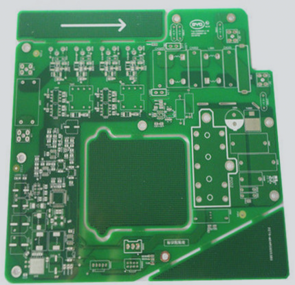
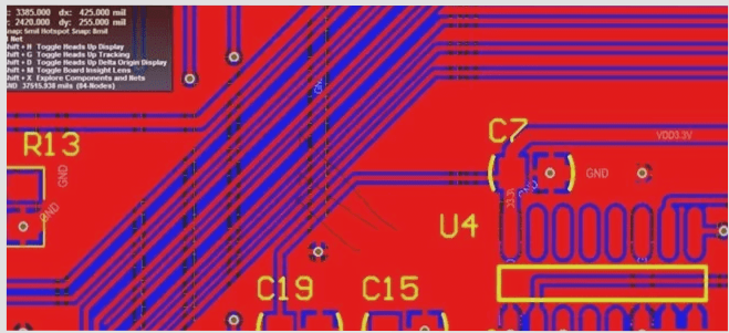
In PCB reverse engineering research, the reverse push principle diagram illustrates the process of deriving information from the PCB document diagram or directly creating the PCB circuit diagram based on the actual product. This approach aims to elucidate the principles and operating conditions of the circuit board. Furthermore, this circuit diagram serves as a tool for analyzing the functional characteristics of the product itself. In forward design, standard product development typically begins with schematic design, followed by PCB design based on that schematic.

Whether for analyzing circuit board principles and product operating characteristics during reverse engineering, or for serving as a foundation in forward PCB design, PCB schematics hold a unique significance. So, how can one effectively reverse-engineer a PCB schematic based on a file diagram or the actual physical object, and what details should be considered throughout the reverse calculation process?
1. **Reasonable Division of Functional Areas**
When undertaking the reverse design of a well-crafted PCB schematic, a sensible division of functional areas can aid engineers in minimizing unnecessary complications and enhancing drawing efficiency. Generally, components with similar functions on a PCB are clustered together, allowing for a convenient and precise basis for inverting the schematic diagram. However, this division is not arbitrary; it requires engineers to possess a solid understanding of electronic circuit principles. Start by identifying the core component within a functional unit, then trace the wiring connections to discover other components of the same unit, thereby establishing functional partitions. This division forms the foundation for schematic drawing. Additionally, engineers should leverage the serial numbers of components on the circuit board, as these can expedite the functional partitioning process.
2. **Correctly Distinguish Lines and Draw Wiring Reasonably**
Engineers must also possess knowledge regarding power supplies, circuit connections, and PCB wiring to accurately distinguish between ground, power, and signal lines. This distinction can be analyzed through the connections of components, the width of copper traces, and the characteristics of the electronic product itself. To prevent line crossings and intermingling, a multitude of ground symbols can be employed for ground lines. Utilizing different colors and line styles for various connections ensures clarity and easy identification. For individual components, special symbols can be introduced, or unit circuits can be drawn separately and later combined.
3. **Find the Right Reference Parts**
The reference parts can be considered the primary components used at the onset of schematic drawing. Once identified, the schematic can be constructed around the pins of these reference components, which enhances the accuracy of the drawing. For engineers, selecting reference parts is typically straightforward. Generally, key components within the circuit—often larger in size and with multiple pins—are ideal choices. Examples include integrated circuits, transformers, and transistors, all of which serve as suitable reference components.
4. **Master the Basic Framework and Learn from Similar Schematic Diagrams**
Engineers need to be proficient in the basic composition of electronic circuit frameworks and the methods of principle drawing. This knowledge allows them to draw not only simple, classic unit circuits but also to develop the overall structure of electronic circuits. Additionally, it’s important to recognize that similar types of electronic products often share schematic similarities. Engineers can draw on their experience and learn from comparable circuit diagrams to effectively reverse-engineer the schematics of new products.
5. **Verification and Optimization**
Once the schematic drawing is complete, the reverse design of the PCB schematic is essentially finished after rigorous testing and validation. It’s crucial to check and optimize the nominal values of components sensitive to PCB distribution parameters. By comparing and analyzing the schematic against the PCB documentation, engineers can ensure full consistency before proceeding with sample board testing.
—
Feel free to ask if you need further modifications!


