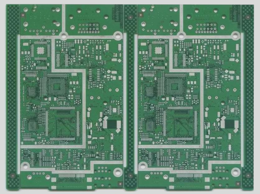
The Importance of Through-Hole Structures in Modern PCB Design
With the increasing use of fine-pitch devices and smaller PCBs, through-hole structures within pads have become essential in modern PCB design. These structures play a crucial role in enhancing the overall performance and functionality of printed circuit boards.
Advantages of Through-Hole Technology
- Allows for tighter component packaging
- Enhances thermal management
- Reduces parasitic inductance and capacitance

The Role of HDI Boards and Micro Blind Buried Hole Technology
As wiring density in product designs continues to rise, HDI boards and micro blind buried hole technology are becoming increasingly prevalent. These technologies address the challenges posed by higher-order vias and contribute to improved signal speed and circuit board component density.
Key Points about Vias in PCB Design
- Vias establish electrical connections between different layers
- Through holes act as vertical wiring within a PCB
- VIPPO and SKIPPO are common methods used for via placement
The use of VIPPO technology, including VIPPO vias and electroplated pad through holes, offers numerous benefits in terms of routing efficiency, heat dissipation, and inductance reduction in high-frequency PCBs.
Advantages of VIPPO Technology
- Enhances routing efficiency by providing holes on the solder pad
- Assists in heat dissipation through holes in the pad
- Reduces inductance in high-frequency PCBs with holes on the solder pads
- Offers a flat surface for components through holes in the pad
VIPPO technology, with its unique features and applications, is particularly well-suited for high-end products like communication devices and servers.