A DC-to-DC converter is one of the most widely used circuits in electronics, especially in power supply applications. The three main types of non-isolated DC-to-DC converters are Buck, Boost, and Buck-Boost. A buck converter is often referred to as a step-down converter, while a boost converter is called a step-up converter.
In this article/video, I present an adjustable 5A DC-to-DC converter circuit that utilizes an advanced chip from Texas Instruments, the TPS5450. This high-frequency, efficient buck converter chip offers precise voltage regulation. I followed several PCB design best practices to ensure low noise, minimal EMI, and high output voltage stability.
For the schematic and PCB design, I used Altium Designer 23 and shared the project with my colleagues via Altium-365. The fast component search engine, Octopart, enabled me to quickly access component information and generate the BOM. To ensure high-quality fabricated boards, I sent the Gerber files to Wellcircuits and tested the circuit’s output stability and noise using a DC load, multimeter, and oscilloscope. Soon, I will also conduct a step-response test and share the results.
Download the Gerber files or order 10 high-quality boards for just $5 USD
If you prefer a fully assembled PCB (including free shipping), click here to order.
Specifications
Input Voltage: 5.5V to 36V
Output Voltage: 1.22V (min) to 31V (max) (adjustable)
Continuous Output Current: 5A
Peak Output Current (short duration): 6A
Maximum Output Voltage Drop: 22mV (at 5A load)
Output Noise: 14mVp-p (no load), 50mVp-p (5A load), 20MHz-BW
Circuit Analysis
Figure 1 illustrates the schematic of the device. As shown, the core of the circuit is IC1 [1], a sophisticated buck converter chip from Texas Instruments.
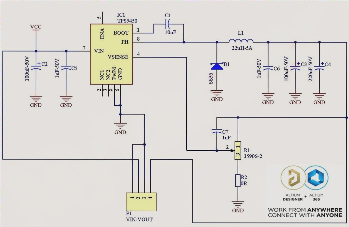
Figure 1
Schematic diagram of the 5A Adjustable Switching Power Supply (Altium)
C2 and C5 are input bypass capacitors and are critical components for stable operation. Please refer to the YouTube video for more details on PCB design rules. IC1 is the heart of the circuit. According to its datasheet: “The TPS5450 is a high-output-current PWM converter with an integrated low-resistance, high-side N-channel MOSFET. It features a high-performance voltage error amplifier that ensures tight voltage regulation even under transient conditions. Other features include an undervoltage lockout to prevent startup until the input voltage exceeds 5.5V, an internally set slow-start circuit to limit inrush currents, and a voltage feedforward to improve transient response. The ENA pin reduces the shutdown supply current to 18μA typically. Additional protections include overcurrent limiting, overvoltage protection, and thermal shutdown. The feedback loop is internally compensated to simplify design and reduce external component count.”
D1 is a SS56 Schottky diode [2]. Along with D1, L1, and IC1, it forms the essential components of the buck converter. C3, C4, and C6 are output capacitors designed to minimize noise.
R1 is a 5K potentiometer [3] used to adjust the output voltage. To maintain full control over the output voltage range from 1.2V to 31V, R2 should be set to zero (using a 0R-0805 resistor). However, if you want to limit the maximum output voltage, you can use a resistor for R2. For example, by using a 5K potentiometer and a 470Ω resistor for R2, the maximum output voltage would be around 14.5V. These values are suitable if you plan to use the power supply in the range of 1.2V to 12V. Using R2 allows for finer control over the voltage range, enabling precise adjustment of the potentiometer. You can adjust R2 to achieve other output voltages with just a few trials.
PCB Layout
Figure 2 shows the PCB layout of the design. It is a compact two-layer PCB, with the bottom layer acting as a solid ground plane. Figure 3 provides a 3D view of the PCB and the assembly drawings.
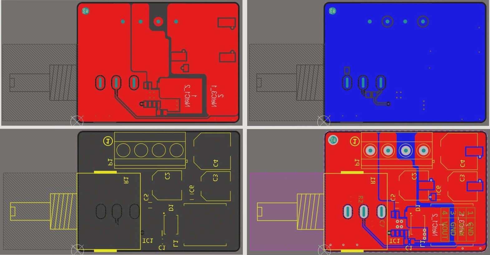
Figure 2
PCB layout of the 5A Adjustable Switching Power Supply
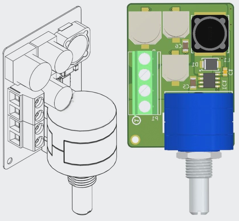
Figure 3
3D view of the PCB and assembly drawings
Test and Verification
There are three key tests to evaluate the performance of a buck converter: line/load regulation, output noise, and step-response test. Please watch the video for detailed explanations. The converter board demonstrated a voltage drop of approximately 10mV under a 3A load. Figure 4 shows the output noise with no load, while Figure 5 shows the noise under a 3A load (using a DC load). This noise can be further reduced by adding decoupling capacitors close to the load.
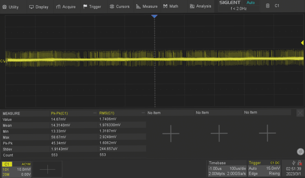
Figure 4
Output noise of the power supply (no load)
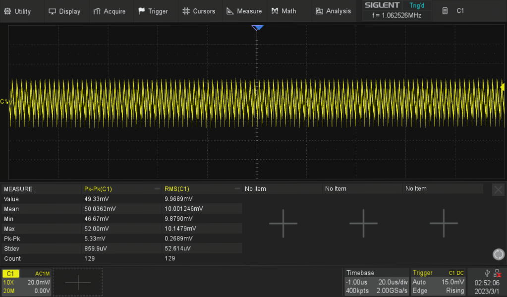
Figure 5
Output noise of the power supply (maximum load, 5A)
Bill of Materials
Figure 6 shows the bill of materials (BOM) for the project. Octopart is not only a fast search engine for electronic components but also an excellent tool for creating BOMs for free.
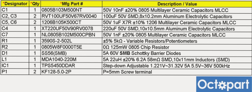
Figure 6
Bill of materials for the 5A-35V Adjustable Switching Power Supply

