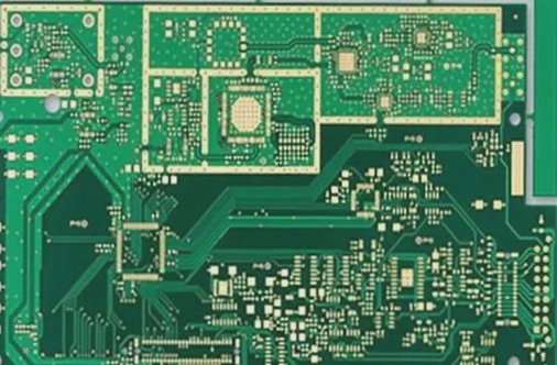
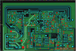
The Importance of PCB Board Design in Modern Digital Systems
With the rapid advancement of digital technology in various fields such as communications, video, networking, and computing, the quality of printed circuit boards (PCBs) plays a critical role in ensuring optimal system performance. As signal frequencies increase and pulse rise times shorten, the demand for high-quality PCB designs has never been greater.
Understanding Crosstalk in PCB Design
One of the key challenges in modern PCB board design is managing crosstalk, which can lead to issues like increased noise levels, signal reflections, and jitter on data edges. By utilizing transmission line theory and considering factors such as edge connectors, microstrip lines, and component sockets, PCB designers can model and mitigate crosstalk effectively.
Methods for Studying Crosstalk
- 1) Achieving the rated impedance value by balancing capacitive and inductive reactance is crucial for minimizing crosstalk in PCB designs.
- 2) Components, connectors, and terminations on the circuit board determine the impact of crosstalk on overall performance.
- 3) Time domain measurements help in analyzing crosstalk by calculating corner frequencies and understanding the PCB board crosstalk model.
Frequency Domain vs. Time Domain Measurements
- 4) While frequency domain techniques are commonly used to observe harmonic components, time domain measurements provide insights into crosstalk by analyzing digital signal edges.
- 5) Correlating signal speed with frequency components aids in understanding crosstalk mechanisms and determining the corner frequency.
Enhancing System Reliability
Designers must analyze circuit performance below the knee frequency to ensure reliable operation of digital systems. Understanding the PCB board crosstalk model and different types of crosstalk mechanisms is essential for minimizing interference.
Types of Crosstalk and Coupling Mechanisms
- 6) Mutual impedance between microstrip lines can lead to crosstalk, with forward and reverse types affecting signal propagation in different ways.
- 7) Forward crosstalk accumulates voltages at the victim line, while reverse crosstalk manifests as low-level wide pulse signals at the source end of the interfered line.
Conclusion
By understanding the complexities of crosstalk in PCB designs and employing appropriate mitigation strategies, designers can enhance system reliability and performance in modern digital systems.

Effective Crosstalk Measurement
To accurately measure crosstalk, it is essential to use a wideband oscilloscope with a bandwidth of at least 20 GHz. This oscilloscope should be paired with a high-quality pulse generator that matches the rise time of the oscilloscope. Additionally, using high-quality cables, terminations, and adapters is crucial for ensuring precise testing of the PCB under examination.
Forward Crosstalk Measurement
When conducting forward crosstalk measurements, it is important to terminate all traces to eliminate reflections. The measurement should be taken at the end of a well-terminated victim wire, as shown in Figure 6.
Impact of Circuit Design on Crosstalk
Despite efforts to reduce crosstalk through meticulous PCB board design, residual effects may still be present. Integrating appropriate end-of-line loads in the circuit design can help reduce crosstalk and minimize its long-term impact.