DC-DC Boost Converter Design Guide
DC-DC converters play a crucial role in various projects and industries. The three main types of non-isolated DC-DC converters are buck, boost, and buck-boost. Today, we will focus on a compact DC-DC boost converter design using popular components like the UC3843 PWM controller, a Schottky diode, and an N-channel MOSFET. This design is perfect for converting 12V to 18V, making it ideal for powering devices like laptops from a single 12V battery.
Latest Updates:
- Input Voltage: 9-16V
- Output Voltage: Up to 28V (adjustable)
- Output Current: Maximum 4A
- Output Noise (no load): 5mVrms
- Output Noise (2A load): 27mVrms
Circuit Analysis
Figure 1 illustrates the schematic of the UC3843-based DC-DC boost converter. The core component here is the UC3843 chip, responsible for controlling the power conversion process.
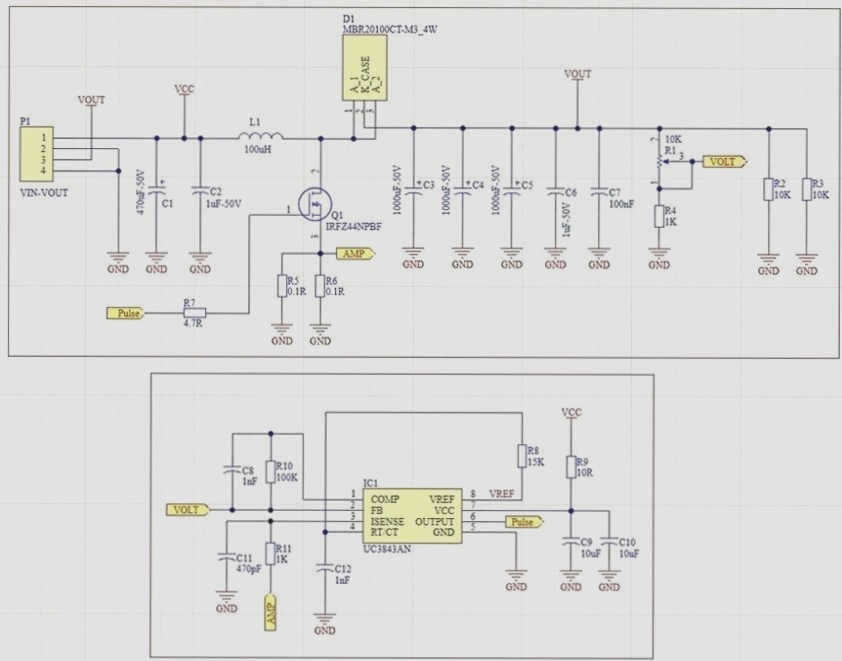
Schematic diagram of the UC3843-based DC-DC boost converter
The UC3843 PWM controller, along with components like C1, C2, L1, D1, and Q1, form the boost converter network. These components are carefully selected for optimal performance in this design.
To reduce output noise, capacitors C3, C4, C5, C6, and C7 are integrated. It’s worth noting that boost converters tend to generate more noise compared to buck converters, especially when using discrete components.
R1, a 10kΩ multi-turn potentiometer, allows for precise adjustment of the output voltage. The output voltage can be calculated using the formula: Vout = 2.5 (1 + R1/R5).
For stability and voltage control, resistors R2 and R3 are utilized as a parallel load. It’s essential to be cautious when adjusting the output voltage to avoid exceeding component tolerances.
PCB Layout
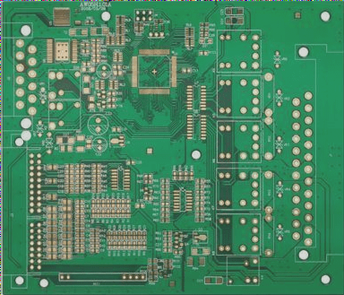
Figure 2 showcases the PCB layout for the DC-DC boost converter. This double-sided PCB includes a mix of SMD and through-hole components, providing a comprehensive view of the top and bottom layers, silkscreen, and solder mask (top layer).
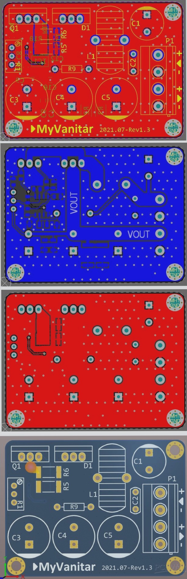
PCB layout for the DC-DC boost converter
During the design phase, utilizing SamacSys component libraries within Altium Designer proved invaluable, ensuring accuracy and efficiency in component selection and placement.
Supported PCB Design Software with SamacSys Plugins
When working on a PCB project, utilizing SamacSys libraries can greatly enhance your design process. These libraries provide essential components like IC1, Q1, and D1, as referenced in your project. If needed, you also have the option to download component libraries from componentsearchengine.com and import them manually. Figure 4 visually represents the components chosen within the SamacSys Altium plugin.
Selected Components in the SamacSys Altium Plugin
For a seamless PCB design experience, the SamacSys Altium plugin allows you to select and integrate components effortlessly. This plugin streamlines the process of choosing components, enhancing the efficiency of your design workflow.
Assembly and Testing
As depicted in Figure 5, the assembled PCB provides a comprehensive view from both the top and bottom angles. This prototype incorporates two parallel resistors in the final revision to function as a preliminary load. The PCB utilizes a combination of through-hole and SMD components, ensuring a balance between ease of assembly and functionality. If desired, you also have the option to order a pre-assembled board for convenience.
When assessing voltage regulators, two crucial parameters to consider are line regulation and load regulation. Line regulation focuses on the power supply’s capability to maintain a consistent output voltage despite fluctuations in the input voltage. On the other hand, load regulation pertains to the power supply’s ability to sustain the output voltage within specified limits despite variations in the load. These parameters are typically evaluated using a DC load. Currently, I am anticipating the delivery of the Siglent SDL1020X-E DC load [10] to perform detailed tests on this converter. In the meantime, I have conducted measurements on the output noise levels.
Output Noise Analysis
Figure 6 showcases the output noise levels under no-load conditions, measured utilizing the Siglent SDS2102X Plus oscilloscope [11]. The waveform exhibits some high-frequency spikes, which are likely attributed to long signal paths or other factors. Analyzing and mitigating these noise levels is crucial for ensuring the stability and performance of the PCB design.