Understanding Parasitic Elements in PCB Boards
When designing PCB boards, it’s essential to consider the impact of parasitic elements on system behavior. While circuit diagrams provide a basic understanding, they often overlook crucial details found in the actual PCB layout. Parasitic elements, such as resistors, capacitors, and inductors, play a significant role in determining signal behavior in complex systems.
What Are Parasitic Elements?
Parasitic elements are components that are not explicitly included in circuit diagrams but have a substantial effect on system performance. These elements, which include factors like DC resistance, parasitic capacitance, and parasitic inductance, can lead to unexpected signal behavior in PCB boards and ICs. Understanding and modeling parasitic elements are crucial for predicting and addressing system issues.
Factors Influencing Parasitic Elements
- Geometry: The layout and arrangement of conductors on the PCB board impact parasitic elements like capacitance and inductance.
- Dielectric Constant: The dielectric constant of the PCB material affects parasitic capacitance between components.
- Permeability: Magnetic components, such as ferrite transformers, contribute to parasitic inductance and affect signal behavior.
- Frequency: Parasitic effects are frequency-dependent, requiring consideration of signal behavior across different frequencies.
Challenges in Modeling Parasitic Elements
While Linear Time-Invariant (LTI) systems cover most practical electrical systems, modeling nonlinear and time-varying parasitic elements can be complex. Factors like fiber weaving effects and transmission line behaviors pose challenges in accurately simulating parasitic elements. However, tools like SPICE simulation can help in analyzing frequency-dependent behavior and identifying potential issues in PCB layouts.
Conclusion
By recognizing and accounting for parasitic elements in PCB designs, engineers can optimize system performance and reduce the risk of unexpected behavior. Understanding the impact of parasitics is essential for creating reliable and efficient electronic systems.
Understanding Ground Bounce in Integrated Circuits
The schematic below illustrates a common circuit model used to analyze ground bounce in integrated circuits. Ground bounce is caused by parasitic inductance in the ground wire (labeled L in the schematic). In addition to inductance, other factors such as parasitic capacitance and resistance influence the circuit’s behavior in the presence of ground bounce.
Extracting Parasitic Effects
Parasitic extraction aims to estimate the frequency-dependent behavior of a system by identifying capacitive or inductive elements across specific frequency ranges. By comparing simulation results with experimental data obtained through frequency sweeps or transient analysis, parasitic effects can be identified and analyzed.
Methods for Parasitic Extraction
- Analytical Methods: Utilize equations to calculate the frequency-dependent behavior of circuit models based on component values from data sheets or experience.
- Regression Method: Employed when equivalent values of parasitic elements are unknown, using regression techniques to compare model predictions with measured data.
Running PSpice Simulations
In PSpice simulations, varying parasitic values and frequencies can help build models that describe circuit behavior. By setting global parameters and analyzing simulation data, parasitic inductance and resistance can be extracted for accurate modeling.
Extracting Parasitic Capacitance
For instance, extracting parasitic capacitance involves identifying the self-resonant frequency of a capacitor affected by series resistance and inductance. By sweeping frequencies and parameter values, simulations can reveal self-resonant frequency and ESL values, aiding in accurate parasitic extraction.
Utilizing Simulation Data
Simulated and measured impedance data can be compared to refine models and calculate precise parasitic values. Adjusting models based on observations allows for accurate prediction of parasitic effects in circuit designs.
Optimizing Circuit Layout
Consideration of parasitic elements and accurate extraction techniques enhance circuit design and layout optimization for improved performance.
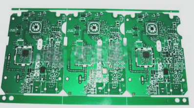
The Challenge of Extracting Parasitics in Complex PCB Board Layouts
As PCB board layouts become increasingly intricate, extracting parasitic elements through equivalent circuit modeling can pose a significant challenge. While it is possible to develop a program to iteratively fit data to a predefined experimental model, accurately determining the nature of the parasitic elements and their corresponding circuit configuration (whether parallel, series, or more complex) remains a daunting task.
One alternative approach involves reverting to a field solver to extract parasitics from the PCB board layout. This method simplifies the process by allowing users to select the interconnects for analysis and utilize an automatic extraction tool. By leveraging Maxwell’s equations, the integrated field solver can directly calculate the equivalent parasitic elements within the PCB board layout, offering a more straightforward solution to this intricate problem.