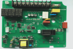
Improving PCB Quality Through Enhanced Manufacturing Processes
In the competitive PCB industry, manufacturers are constantly striving to improve product quality while reducing costs. By focusing on eliminating defects and enhancing production processes, companies aim to gain a competitive edge by offering superior quality at competitive prices.
Identifying Defects and Causes
1. Coating Pitting Issue:
One common defect observed in PCBs is coating pitting, which manifests as pockmarks on the patterned copper electroplating, especially at the board’s center. This issue can be attributed to several factors:
- Improper treatment of the electroplating copper solution with activated carbon
- Inadequate filtration and circulation of the solution
- Direct treatment of phosphor copper anodes without electrolytic processing
These factors lead to rough and pitted coatings, impacting the overall quality of the PCBs. To address this issue, it is essential to adhere strictly to documented process procedures and ensure proper electrolytic treatment of anodes.

Efforts to troubleshoot the coating pitting problem included replacing the filter element in the electroplating solution and conducting electrolysis on anodes from multiple tanks. These measures resulted in improved PCB characteristics, highlighting the importance of meticulous process management in PCB manufacturing.
2. Coating Bloom (Dendritic) Issue:
Another common problem in PCBs is coating bloom, also known as dendritic growth. This issue can arise due to various factors, such as contaminated plating solutions or inadequate cleaning processes. Addressing coating bloom requires thorough monitoring of plating solutions and strict adherence to cleaning protocols.
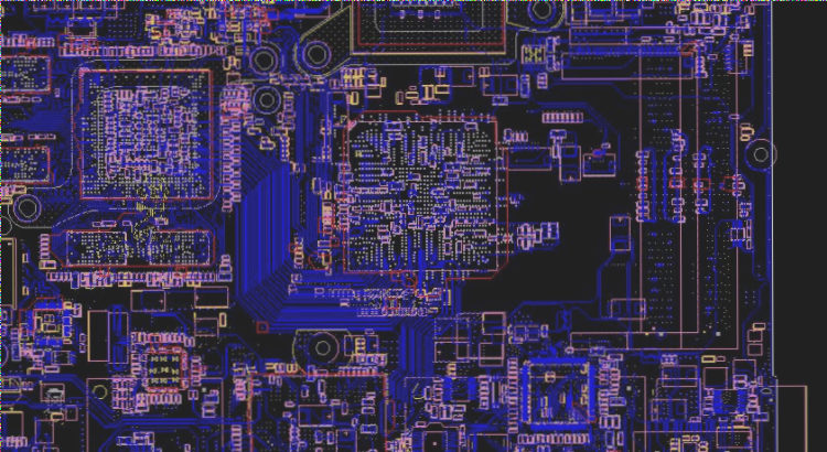
Patterned Copper Electroplating in PCB Fabrication
The floral pattern seen on the surface of patterned copper electroplating is a common occurrence, especially over large areas. However, when it comes to PCB boards with pads or thin lines plated on the same day, the presence of defects is minimal.
Initially, the coating bloom phenomenon was not given much attention and was considered incidental. Subsequent investigation, however, revealed that PCB boards, particularly those labeled MON?_1 (measuring 265mm x 290mm with an A surface area of 2.35dm2 and a B surface area of 4.48 dm2), exhibited significant coating bloom issues. This has a substantial impact on the appearance of the PCBs, leading to the production of numerous defective boards that require thorough analysis to identify and rectify the faults.
With a focus on customer satisfaction, our quality department is committed to identifying and intercepting all PCB boards with defective coatings, whether it be extensive bloom or filamentous traces on the lines. Quality remains our top priority, and our technical team is dedicated to investigating and resolving any coating issues that may arise.