Designing a Solar Power Regulator PCB: A Beginner-Friendly Project
Designing a solar power regulator PCB is essential for optimizing the efficiency of your solar panels. This project aims to guide beginners through the process, ensuring maximum power output and efficient charging.
Required Components for the Project
Before starting, make sure you have all the necessary components for the project.

Background Information
In modern solar energy systems, Maximum Power Point Tracking (MPPT) technology is crucial for optimizing solar panel charging. However, in low-light conditions, a dedicated solar charger like the LT3652 becomes essential to maintain efficiency.

How the LT3652 Works
The LT3652 is a highly efficient DC-to-DC converter that optimizes energy conversion from solar panels to batteries. Here’s how it works:
- The LT3652 converts DC power from solar panels into high-frequency AC and then back to the required DC voltage for the battery.
- Input regulation ensures peak power output from the solar panel, maximizing energy conversion.
- It automatically stops charging when the current drops below a certain threshold, protecting the battery and panel.
Schematic Diagram
The schematic diagram showcases how the LT3652 integrates into the design for effective solar battery charging.
- The barrel jack acts as a switch, allowing seamless connection of external batteries for continuous charging.
- Designed using KiCAD EDA, the schematic ensures precise circuit layout for optimal performance.

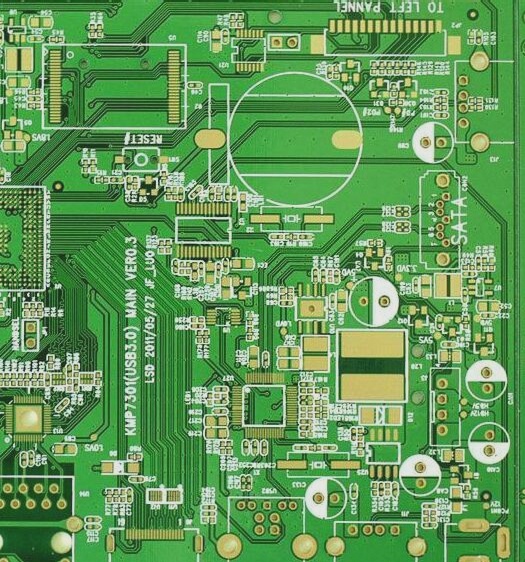
PCB Design
After finalizing the schematic, the design transitions into a PCB layout for manufacturing.
- Specify component dimensions and board size according to project requirements during the design phase.
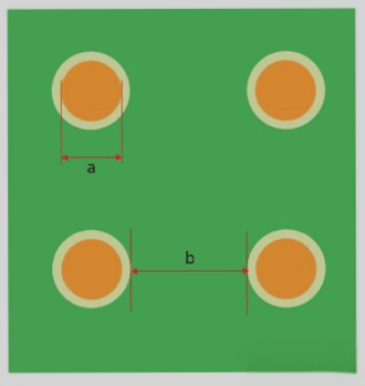
- KiCAD’s design rule checks (DRC) ensure error-free PCB layout, preventing issues during manufacturing.
- Thoroughly check all connections to avoid damage to components like solar panels and batteries.

Design Manufacturing
After finalizing the design, the next step is fabrication, where a PCB manufacturer produces the physical board based on your design files.
- Consider WellCircuits for reliable PCB manufacturing services.
- Submit the necessary manufacturing files, including Gerber files, BOM, and Pick-and-Place files.
Bill of Materials (BOM)
The Bill of Materials (BOM) is essential for ordering components needed to assemble your PCB, generated directly from your design tool.
Creating BOM File in KiCAD
- Go to File, select Fabrication Output, and choose BOM.
Generating the BOM file in Excel format allows for easy editing to meet specific manufacturer requirements.

Generating Gerber Files
Follow these steps to create Gerber files for PCB manufacturing:
- Click on the icon to open the plot window, then select “Plot” to generate the Gerber files.

Upon completion, your Gerber files will be ready for submission to the manufacturer.

For further inquiries regarding PCB or PCBA, please reach out to us at info@wellcircuits.com.