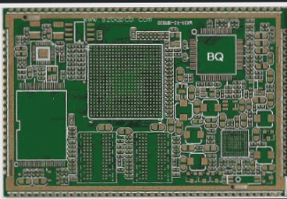
Antenna PCBs in Wireless Devices
Antenna PCBs play a crucial role in telecommunications for signal transmission and reception. With the rise of 5G networks, the demand for antenna PCBs has surged, especially in Internet of Things (IoT) applications.

PCB Board Antenna Functionality
A PCB board antenna is responsible for wireless signal transmission and reception. It converts high-frequency currents into electromagnetic waves for transmission and vice versa for reception. The advantages of PCB board antennas include space efficiency, cost-effectiveness, and ease of integration. However, there are trade-offs such as performance limitations and susceptibility to interference.
Materials for Antenna PCBs
Materials like Rogers PCB, Teflon, and Arlon are commonly used for manufacturing antenna PCBs due to their high-frequency performance. Designing an effective antenna is crucial for radiating RF signals into free space, with considerations for platform characteristics and environmental factors.
Designing a PCB Board Antenna
Antenna PCB design and RF layout are vital for wireless devices. Different antenna designs can significantly impact RF performance. Compact PCB board antennas are essential for many electronic applications, with proper RF grounding and impedance matching being key considerations.
Factors Affecting GPS Antenna Performance
- Ceramic Chip Quality: The quality of ceramic chips affects performance, with larger chips offering better reception.
- Silver Layer: The silver layer on ceramic antennas impacts resonant frequency and may require adjustments for optimal reception.
- Feed Point: The feed point of the ceramic antenna is crucial for signal collection and transmission.
- Amplification Circuit: The PCB board shape carrying the ceramic antenna and amplifier circuit design influence performance, with considerations for gain and signal saturation.


 العربية
 简体中文
简体中文 Nederlands
 English
 Français
 Deutsch
 Italiano
 日本語
日本語 한국어
한국어 Português
 Русский
 Español
 ไทย
ไทย