1. Printed circuit boards, commonly referred to as PCBs, serve as essential providers of electrical connections for electronic components.
2. Their development spans over a century; the primary focus in their design is layout optimization.
3. One of the key advantages of utilizing circuit boards is the significant reduction in wiring and assembly errors, leading to enhanced automation and improved production labor efficiency.
4. With the ongoing advancement of PCB technology, the industry has experienced rapid growth.
5. Concurrently, product competition has intensified, ushering the PCB sector into an era characterized by slim profit margins.
6. For companies to thrive amidst this competition, ensuring manufacturability and effective cost control is crucial.
7. However, gaining competitive advantages through technology and craftsmanship has become increasingly challenging.
8. Engineering design plays a pivotal role at the forefront of the product manufacturing process.
9. It is essential to carefully consider material costs during product design while still meeting customer requirements.
10. Additionally, the manufacturing process must be carefully managed to avoid overwhelming production capacities and to ensure a smooth workflow.
11. Below, we will outline strategies for reducing costs in the PCB manufacturing process.

**1. Printed Circuit Board Size Optimization**
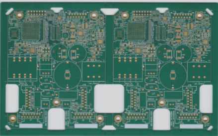
Generally speaking, smaller printed circuit board (PCB) sizes lead to lower costs, although this relationship is not strictly linear. It is influenced by the PCB manufacturing cutting processes. Therefore, when estimating PCB sizes before design, it is crucial to confirm the pricing for each size with the purchasing department first, and then select the most economical size that meets the requirements.
**2. The optimal imposition size for the processing board can be determined based on order type, processing capability, and operational skills.**
Optimizing the imposition size can enhance material utilization, improve efficiency, and reduce water and electricity consumption. However, it may also introduce challenges such as handling issues, scratching, operational difficulties, and a temporary increase in the scrap rate, complicating quality control. The engineering review should be grounded in practical considerations to establish the ideal processing board size.
**3. When initiating the PCB layout design,**
in addition to the architectural design that aligns with functional requirements, it is essential to consider the following factors to save costs: Evaluate whether the same circuit design can be adapted for multiple similar products. Differences in PCB size, target markets, functionalities, and product positioning can necessitate varying designs. If the wiring designs of two PCBs differ only slightly, it is necessary to apply for separate designs, which incurs additional costs. Furthermore, upon completion of the PCB design, each board must undergo reliability and electrical performance testing to ensure product quality, adding extra expenses for prototyping and testing.
**4. Moreover, if the original copper-clad board size is too large, processing can become cumbersome,**
and in some cases, it may not fit into PCB processing equipment at all. Therefore, it is essential to cut it into smaller, manageable processing-size copper-clad boards. The specific processing size must be determined based on the equipment used for PCB fabrication, the dimensions of each PCB, and various process parameters. Besides the length and width required for the printed circuit pattern, these parameters also include the width needed for screw holes to secure the PCB within the electronic product frame, allowances for shape processing, electroless plating, electroplating, and the clearance required for clamps. Additionally, it encompasses the positioning pins for multilayer PCBs, alignment marks between layers, manufacturer logos, and the edge width of the PCB. Recommended process parameter values can often be sourced from copper-clad laminate manufacturers or distributors. During PCB production, this data aids in determining how many processing-size pieces can be cut from a large original copper-clad laminate, whether the cuts are vertical or horizontal, and whether cutting is feasible.
If you have any PCB manufacturing needs, please do not hesitate to contact me.Contact me
2. Their development spans over a century; the primary focus in their design is layout optimization.
3. One of the key advantages of utilizing circuit boards is the significant reduction in wiring and assembly errors, leading to enhanced automation and improved production labor efficiency.
4. With the ongoing advancement of PCB technology, the industry has experienced rapid growth.
5. Concurrently, product competition has intensified, ushering the PCB sector into an era characterized by slim profit margins.
6. For companies to thrive amidst this competition, ensuring manufacturability and effective cost control is crucial.
7. However, gaining competitive advantages through technology and craftsmanship has become increasingly challenging.
8. Engineering design plays a pivotal role at the forefront of the product manufacturing process.
9. It is essential to carefully consider material costs during product design while still meeting customer requirements.
10. Additionally, the manufacturing process must be carefully managed to avoid overwhelming production capacities and to ensure a smooth workflow.
11. Below, we will outline strategies for reducing costs in the PCB manufacturing process.
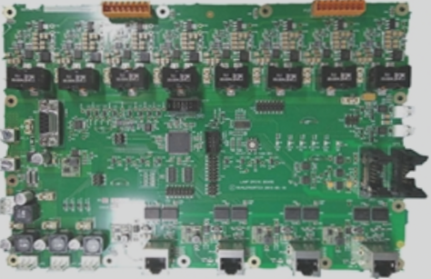
**1. Printed Circuit Board Size Optimization**
Generally speaking, smaller printed circuit board (PCB) sizes lead to lower costs, although this relationship is not strictly linear. It is influenced by the PCB manufacturing cutting processes. Therefore, when estimating PCB sizes before design, it is crucial to confirm the pricing for each size with the purchasing department first, and then select the most economical size that meets the requirements.
**2. The optimal imposition size for the processing board can be determined based on order type, processing capability, and operational skills.**
Optimizing the imposition size can enhance material utilization, improve efficiency, and reduce water and electricity consumption. However, it may also introduce challenges such as handling issues, scratching, operational difficulties, and a temporary increase in the scrap rate, complicating quality control. The engineering review should be grounded in practical considerations to establish the ideal processing board size.
**3. When initiating the PCB layout design,**
in addition to the architectural design that aligns with functional requirements, it is essential to consider the following factors to save costs: Evaluate whether the same circuit design can be adapted for multiple similar products. Differences in PCB size, target markets, functionalities, and product positioning can necessitate varying designs. If the wiring designs of two PCBs differ only slightly, it is necessary to apply for separate designs, which incurs additional costs. Furthermore, upon completion of the PCB design, each board must undergo reliability and electrical performance testing to ensure product quality, adding extra expenses for prototyping and testing.
**4. Moreover, if the original copper-clad board size is too large, processing can become cumbersome,**
and in some cases, it may not fit into PCB processing equipment at all. Therefore, it is essential to cut it into smaller, manageable processing-size copper-clad boards. The specific processing size must be determined based on the equipment used for PCB fabrication, the dimensions of each PCB, and various process parameters. Besides the length and width required for the printed circuit pattern, these parameters also include the width needed for screw holes to secure the PCB within the electronic product frame, allowances for shape processing, electroless plating, electroplating, and the clearance required for clamps. Additionally, it encompasses the positioning pins for multilayer PCBs, alignment marks between layers, manufacturer logos, and the edge width of the PCB. Recommended process parameter values can often be sourced from copper-clad laminate manufacturers or distributors. During PCB production, this data aids in determining how many processing-size pieces can be cut from a large original copper-clad laminate, whether the cuts are vertical or horizontal, and whether cutting is feasible.
If you have any PCB manufacturing needs, please do not hesitate to contact me.Contact me

