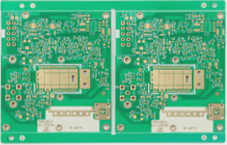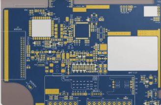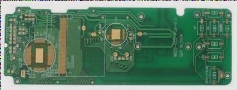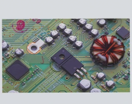
1. PCI-SIG recommends using a four-layer PCB for PCI cards.
2. The signal distribution of PCI connectors specified by PCI-SIG is optimized for the convenience of wiring on a four-layer board.
3. PCI-SIG has also provided a recommended schematic diagram for the pin distribution of PCI controllers.
4. In fact, PCI controller manufacturers like AMCC, PLX, and OXFORD have implemented this recommendation.
5. Under this suggested pin distribution, two layers are utilized, making PCB wiring quite convenient.
6. However, if the PCI card system hardware is complex and requires multiple power split levels, a multi-layer PCB is preferable.
7. Any PCI signal on the PCI card can connect to only one load (including not connecting to a pull-up resistor).
8. Except for CLK, RST, INTA#~INTD#, and JTAG pins, all pins from the golden finger contact point to the load must not exceed 1.5 inches; the CLK signal length is 2.5 ±0.1 inches.
9. This length is relatively long, often necessitating routing adjustments to meet requirements, which is why you frequently see serpentine traces for CLK on PCI cards.
10. There are no specific regulations for the remaining pins.
11. When using a multi-layer PCB, signal traces should not cross different power levels (ideally, the split power level should be on the opposite side of the PCB).
12. This explains why all gold fingers on the A side of the PCI card often route to the B side (component side) through vias.
13. The characteristic impedance for each PCI signal is between 60-100 ohms, with load capacitance not exceeding 10 pF.
14. The IO pad of the IC should withstand -3.5V undershoot and +7.1V overshoot.
15. For PCI controller manufacturers such as AMCC, PLX, and OXFORD, the controller ICs comply with these standards, relieving users from concern.
16. However, if using a CPLD/FPGA for the PCI controller, it’s crucial to verify that the model complies with these specifications.
17. CPLD/FPGA manufacturers like Altera and Xilinx specify in their documentation whether their products meet PCI signal standards.
18. The wiring for a standard 32-bit, 33MHz PCI card is relatively simple, primarily focused on meeting length requirements.
19. While not strictly adhering to wiring requirements typically won’t cause issues, signal compatibility problems may arise depending on the motherboard chipset.
20. When that happens, debugging the hardware of the PCI card can be one of the most challenging experiences in PCB circuit design.


