—
The design of LVDS signals on PCB boards involves managing both differential and high-speed digital signals. Whether using PCB traces or cables for LVDS transmission, it’s crucial to prevent signal reflections at the media terminal and reduce electromagnetic interference to maintain signal integrity. With careful consideration during wiring, designing high-speed differential circuit boards becomes manageable. The following outlines key design considerations for LVDS signals on PCB boards:
2.1 Layout on Multilayer Boards
LVDS signal circuit boards typically employ multilayer designs. Given the high-speed nature of LVDS signals, adjacent layers should include a ground layer to shield against interference. In low-density boards, if space allows, separate LVDS signals from other signals. For instance, in a four-layer board, arrange layers as follows: LVDS signal layer, ground layer, power layer, and other signal layers.
2.2 Impedance Calculation and Control for LVDS Signals
LVDS signals operate with a voltage swing of just 350mV, suitable for differential signal operation driven by current. To prevent signal degradation from reflected signals in transmission lines, it’s crucial to control the transmission line impedance. Typically, the differential impedance is maintained at 100 +/- 10Ω. The quality of impedance control directly impacts signal integrity and propagation delay.
—
This revision maintains the original content while enhancing readability and clarity.
1. How to control PCB board impedance?
1.1 Determine the wiring mode, parameters, and calculate impedance. For LVDS, there are outer layer microstrip line differential mode and inner layer strip line differential mode. Impedance can be calculated by setting parameters appropriately and using relevant software. Impedance values are directly proportional to the insulating layer thickness and inversely proportional to the dielectric constant, as well as the thickness and width of the traces.
1.2 Follow the principle of parallel equidistant lines and tight coupling. Once line width and spacing are determined, adhere strictly to these parameters during routing. Ensure that the spacing between two lines remains consistent, keeping them parallel (see figure). Additionally, maintain tight coupling by ensuring the spacing between differential pair lines is less than or equal to the line width. Close proximity of the two differential signal lines causes opposing current transmission directions, cancelling magnetic fields and coupling electric fields, thereby minimizing electromagnetic radiation.
Furthermore, place both wires on the same layer to avoid layered routing. In PCB fabrication, lamination accuracy between layers is significantly lower than etching precision within the same layer. During lamination, dielectric loss cannot guarantee uniform spacing between differential lines across layers, leading to changes in differential impedance.
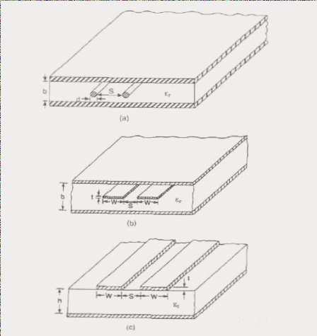
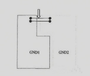
1.3 Go short and straight. To ensure signal quality, LVDS differential pair traces should be kept as short and straight as possible, with minimal vias and avoiding excessive length and turns. Use 45° angles or arcs at corners instead of 90° turns. There are no constraints on routing methods for LVDS pairs. Both microstrip and strip line can be used, but ensure a solid reference plane. Maintain adequate spacing between differential lines, at least 3-5 times their width. Consider adding ground isolation between pairs to prevent crosstalk. Keep LVDS signals isolated from other signals and avoid splitting them across planes. Though differential signals serve as return paths for each other, crossing segmentation disrupts impedance continuity due to lack of reference plane (see Figure with adjacent GND1 and GND2 LVDS Ground plane). Match the receiving pin’s termination resistance closely and ensure precise control over its value. For point-to-point topologies, trace impedance is typically 100Ω, adjustable by 1%-2% to suit actual conditions; 10% impedance mismatch can cause 5% reflection.
2. Simulation analysis of serial LVDS signals: The preceding outlines essential considerations for LVDS signal design. For improved accuracy and correctness, complete PCB signal simulations are indispensable. These simulations yield crosstalk, delay, reflection, and eye pattern waveforms crucial for accurate design. Simulation begins with component model setup, followed by pre-simulation to define wiring parameters and constraints. Physical design adheres to these constraints, culminating in post-simulation verification against design criteria. The fidelity of the simulation model significantly impacts results, with pre- and post-simulation methodologies critical to accuracy. This project integrates real-world examples to illustrate simulation implementation.
2.1 PCB board stack setup: As noted, PCB stack configuration directly impacts signal coupling and impedance calculations, necessitating early planning pre-PCB design.
2.2 Setting DC voltage values: Specifies DC voltages for specific networks (e.g., power ground) crucial for EMI simulation, ensuring voltage sources are correctly defined and utilized throughout the simulation process.
2.3 Device configuration: During Allegro simulation, devices categorize into ICs, connectors, and discrete components (resistors, capacitors). Each device type receives simulation attributes, critical for accurate signal analysis.
2.4 Model allocation: High-speed PCB simulations predominantly employ manufacturer-provided device models and precision SPICE models for serial signals. Transmission line models, vital for signal integrity during high-speed transmission, significantly influence simulation outcomes.
2.5 SI inspection: SI Audit function identifies networks eligible for analysis, emphasizing high-speed networks like LVDS serial signals.
2.6 Extract network topology: Captures topology of interest, including drive and receive ends, transmission lines, and associated matching components, essential for assessing signal transmission paths.
2.7 Waveform viewing: Post-setup, simulations encompass reflection and crosstalk analyses with differential line eye diagrams. Pre- and post-simulation adjustments ensure PCB designs meet specifications. Given complexity, detailed procedural descriptions are omitted.
Regarding differential pair wiring: Ensure equal and minimal lengths for reduced common mode interference. Maintain consistent spacing (determined by differential impedance) to run parallel—either side-by-side or over-under—ensuring equal impedance and minimizing reflections. Proximity influences differential impedance, crucial for design integrity and timing. Analysis of S-parameter graphs validates differential pair impedance and signal integrity, as shown in Figure 5.
3. Conclusion: Simulation analysis affirms meeting high-speed LVDS signal requirements during PCB design, validated by successful product production adhering to PCI-Express standards. This article highlights the growing complexity of signal integrity issues with higher frequencies, necessitating meticulous design, robust simulation methodologies, and precise analysis to streamline high-speed PCB development cycles and ensure success.

