PCB Board Design for Switching Power Supplies
In the realm of switching power supplies, PCB board design plays a crucial role in determining performance, EMC compliance, reliability, and manufacturability. As electronic technology advances, these power supplies are getting smaller, operating frequencies are increasing, and component densities are on the rise.
Anti-Interference Demands in PCB Layout
The demands for anti-interference in PCB layout and wiring are becoming more stringent. A well-planned and scientifically designed PCB layout can significantly enhance efficiency and effectiveness in your work.
Layout Requirements
- Optimal routing efficiency is crucial in PCB layout. Components should be relocated with attention to interconnects and grouped based on related connections.
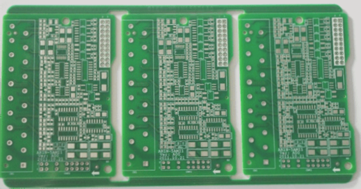
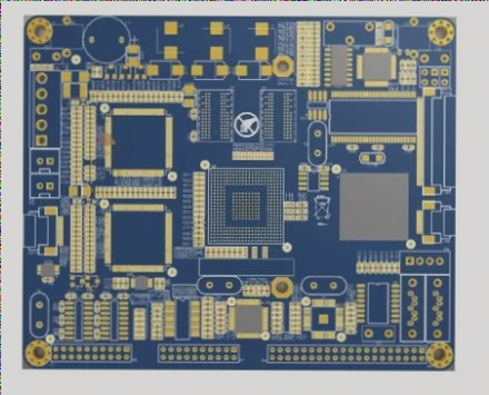
- Arrange components symmetrically and compactly around core functional circuit elements for easier assembly and mass production.
- Consider future soldering and maintenance, avoid component misalignment, and adhere to IPC-A-610E standards.
- Isolate sensitive components from interference sources and minimize loop area for high-frequency currents.
- Strategically place heat-generating elements for even dissipation and consider component height on the bottom layer.
Wiring Principle
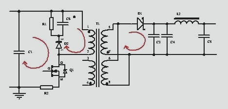
- Separate small signal traces from high-current traces and minimize loop area for critical wiring.
- Avoid lengthy parallel runs and maintain single-point grounding for power and control circuits.
- Segregate high-frequency components and optimize filter capacitor routing for noise-sensitive applications.
By adhering to these principles in PCB board design and layout, you can ensure optimal performance and reliability in switching power supplies.
PCB Design Best Practices for Component Reliability and Safety
1. Enhancing Component Reliability
- Utilize large bare copper areas beneath heat-generating components like TO-252 MOS tubes to improve reliability.
- Use tinned bare copper for high-current flows through narrow power traces.
2. Ensuring Safety Distance and Process Requirements
- Ensure adequate electrical clearance and creepage distance between conductors and adjacent surfaces.
- Utilize isolation slots to enhance primary and secondary isolation, following specific dimensions for safety.
- Maintain a distance between components at the PCB edge to prevent manufacturing issues.
- Implement teardrops for trace widths entering round pads to prevent detachment.
- Provide thermal isolation for SMD device pins connected to large copper areas to avoid soldering issues.
- Consider sub-boarding during PCB assembly to mitigate stress-induced component warping.
By following these guidelines, especially crucial for switching power supplies, PCB designs can optimize functionality and manufacturability.