The Importance of Design in PCB Production
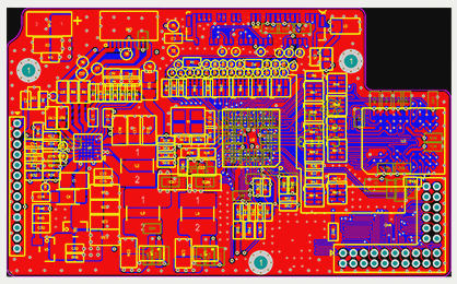
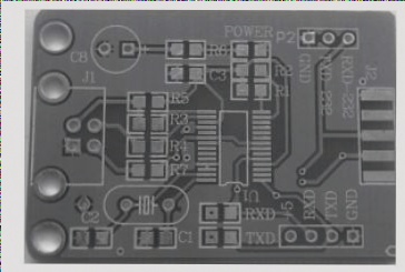
Design plays a crucial role in every step of the circuit board manufacturing process. Achieving high-quality PCB boards involves careful selection, ground wire design, electromagnetic compatibility design, decoupling capacitor configuration, printed circuit board size, device layout, and reliability design like thermal design. These factors are essential for ensuring the reliability and performance of electronic equipment.
Significance of PCB Design
Printed circuit boards remain the primary method for assembling electronic equipment and systems. Even with a correct circuit schematic design, improper PCB layout can greatly impact electronic equipment reliability. For example, placing two thin parallel lines closely on the board can cause signal waveform delays and reflection noise formation at the transmission line’s end. Therefore, adopting the right design approach is crucial when creating a PCB.
Ground Wire Design Considerations
- Single-Point vs. Multi-Point Grounding: In low-frequency circuits (< 1MHz), single-point grounding is recommended to minimize interference. For frequencies above 10MHz, multiple points should be used to reduce impedance. Frequencies between 1 and 10MHz require careful consideration of grounding methods.
- Separation of Digital and Analog Circuits: It is vital to separate high-speed logic circuits from linear circuits on the PCB and avoid mixing their ground wires. Increasing the grounding area of linear circuits is beneficial.
- Thicker Ground Wires: Thin ground wires can lead to ground potential fluctuations, affecting timing signal levels and noise performance. Ground wires should be thick enough to carry current effectively, with a width exceeding 3mm.
- Formation of Closed Ground Wire Loop: Creating a closed loop for ground wires in PCBs with digital circuits enhances anti-noise capabilities. This is particularly important when multiple integrated circuit components are present, reducing potential differences and improving noise performance.
By focusing on proper design practices, including ground wire design considerations, PCB manufacturers can enhance the reliability and performance of electronic equipment, ensuring optimal functionality and reduced interference issues.


