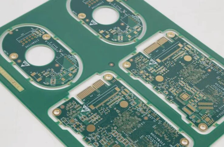
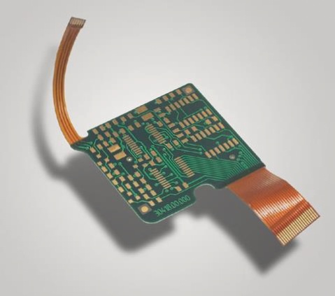
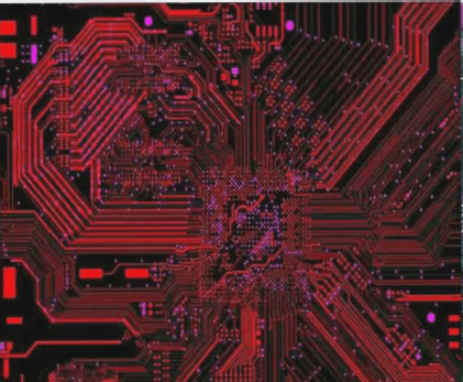
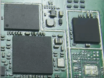
This paper introduces a design method for a high-speed digital signal PCB board based on computer analysis of signal integrity. In this design method, firstly, a signal transmission model at the PCB board level will be established for all high-speed digital signals. Then, the design solution space will be determined through calculation and analysis of signal integrity, and the PCB board will be completed based on the solution space through design and verification.
With the increase in output switching speed of integrated circuits and PCB density, signal integrity has become a critical issue in the design of high-speed digital PCB boards. Factors such as component and PCB board parameters, component layout on the PCB board, and wiring of high-speed signals can lead to signal integrity problems, resulting in unstable system operation or even complete failure. The ability to fully consider signal integrity during the PCB design process and implement effective control measures is a key focus in the PCB design industry today. The high-speed digital PCB design method based on computer analysis of signal integrity can effectively address signal integrity concerns in PCB design.

Overview of Signal Integrity Issues
Signal integrity (SI) refers to the ability of a signal to respond with the correct timing and voltage in a circuit. A circuit has good signal integrity if the signals in the circuit can reach the integrated circuit (IC) with the required timing, duration, and voltage amplitude. Conversely, a signal integrity problem occurs when the signal does not respond properly. Signal integrity problems are mainly manifested in delay, reflection, crosstalk, simultaneous switching noise (SSN), and electromagnetic compatibility (EMI). Delay occurs when the signal is transmitted at a limited speed on the wires of the PCB board, impacting the timing of the system. Reflection happens when the characteristic impedance of the wire on the PCB does not match the load impedance, causing energy to be reflected back along the transmission line. Crosstalk occurs due to mutual capacitance and mutual inductance between devices or wires on the PCB, affecting other devices or wires when a signal changes.
SSN occurs when many digital signals on the PCB are switched synchronously, generating noise on the power and ground lines. EMI, like other electronic devices, is related to the layout and wiring methods of PCB boards.
Traditional PCB Board Design Method
In the traditional design process, the PCB board design includes circuit design, layout design, PCB board production, measurement, and debugging. However, the traditional method lacks effective analysis methods for signal transmission characteristics on the actual PCB board, leading to challenges in selecting appropriate signal topology and component parameters. Quality of layout design is dependent on designer experience, and controlling the performance of the PCB board is difficult due to manufacturing tolerance ranges. This results in long product development cycles and high research and development costs.
PCB Board Design Method Based on Signal Integrity Analysis
The PCB board design process based on signal integrity analysis establishes a model for high-speed digital signal transmission, allowing for pre-analysis of signal integrity problems. The design method integrates component types, parameters, and circuit topology based on simulation results. Flexible design solutions are ensured by analyzing possible parameter changes in the layout design process. Post-design signal integrity analysis confirms if layout design meets requirements, reducing the risk of product failure. This method shortens product development cycles and lowers development costs by minimizing the need for repeated modifications.
Signal Integrity Analysis Model
Establishing a PCB board-level signal integrity model is crucial in the design method based on signal integrity analysis. Three commonly used models for PCB-level signal integrity analysis are SPICE, IBIS, and Verilog-A. SPICE provides accurate simulation but is time-consuming, while IBIS is widely supported by semiconductor manufacturers. Verilog-AMS and VHDL-AMS offer behavior-level modeling but have limited manufacturer support. Selecting models based on component requirements and availability ensures accurate signal integrity analysis.
Combining Design Methods with Existing EDA Software
Presently, there is no integrated EDA software for PCB board design, so a combination of general software tools is needed. SPICE software is used to build models for discrete devices and transmission lines, integrated into signal integrity analysis software such as SPECCTRAQuest. Design constraints are based on simulation results, implemented in general PCB design software like OrCAD. After layout design, parameters are extracted for further signal integrity analysis to verify design requirements. Experimental measurements validate model correctness, ensuring the reliability of the design method for high-speed digital PCB boards.
With the increase in output switching speed of integrated circuits and PCB density, signal integrity has become a critical issue in the design of high-speed digital PCB boards. Factors such as component and PCB board parameters, component layout on the PCB board, and wiring of high-speed signals can lead to signal integrity problems, resulting in unstable system operation or even complete failure. The ability to fully consider signal integrity during the PCB design process and implement effective control measures is a key focus in the PCB design industry today. The high-speed digital PCB design method based on computer analysis of signal integrity can effectively address signal integrity concerns in PCB design.
Overview of Signal Integrity Issues
Signal integrity (SI) refers to the ability of a signal to respond with the correct timing and voltage in a circuit. A circuit has good signal integrity if the signals in the circuit can reach the integrated circuit (IC) with the required timing, duration, and voltage amplitude. Conversely, a signal integrity problem occurs when the signal does not respond properly. Signal integrity problems are mainly manifested in delay, reflection, crosstalk, simultaneous switching noise (SSN), and electromagnetic compatibility (EMI). Delay occurs when the signal is transmitted at a limited speed on the wires of the PCB board, impacting the timing of the system. Reflection happens when the characteristic impedance of the wire on the PCB does not match the load impedance, causing energy to be reflected back along the transmission line. Crosstalk occurs due to mutual capacitance and mutual inductance between devices or wires on the PCB, affecting other devices or wires when a signal changes.
SSN occurs when many digital signals on the PCB are switched synchronously, generating noise on the power and ground lines. EMI, like other electronic devices, is related to the layout and wiring methods of PCB boards.
Traditional PCB Board Design Method
In the traditional design process, the PCB board design includes circuit design, layout design, PCB board production, measurement, and debugging. However, the traditional method lacks effective analysis methods for signal transmission characteristics on the actual PCB board, leading to challenges in selecting appropriate signal topology and component parameters. Quality of layout design is dependent on designer experience, and controlling the performance of the PCB board is difficult due to manufacturing tolerance ranges. This results in long product development cycles and high research and development costs.
PCB Board Design Method Based on Signal Integrity Analysis
The PCB board design process based on signal integrity analysis establishes a model for high-speed digital signal transmission, allowing for pre-analysis of signal integrity problems. The design method integrates component types, parameters, and circuit topology based on simulation results. Flexible design solutions are ensured by analyzing possible parameter changes in the layout design process. Post-design signal integrity analysis confirms if layout design meets requirements, reducing the risk of product failure. This method shortens product development cycles and lowers development costs by minimizing the need for repeated modifications.
Signal Integrity Analysis Model
Establishing a PCB board-level signal integrity model is crucial in the design method based on signal integrity analysis. Three commonly used models for PCB-level signal integrity analysis are SPICE, IBIS, and Verilog-A. SPICE provides accurate simulation but is time-consuming, while IBIS is widely supported by semiconductor manufacturers. Verilog-AMS and VHDL-AMS offer behavior-level modeling but have limited manufacturer support. Selecting models based on component requirements and availability ensures accurate signal integrity analysis.
Combining Design Methods with Existing EDA Software
Presently, there is no integrated EDA software for PCB board design, so a combination of general software tools is needed. SPICE software is used to build models for discrete devices and transmission lines, integrated into signal integrity analysis software such as SPECCTRAQuest. Design constraints are based on simulation results, implemented in general PCB design software like OrCAD. After layout design, parameters are extracted for further signal integrity analysis to verify design requirements. Experimental measurements validate model correctness, ensuring the reliability of the design method for high-speed digital PCB boards.

