Enhancing PCB Board Testing Machine Speed with FPGA-Based Hardware Control System
To improve the testing speed of PCB board testing machines and streamline circuit board design, a hardware control system design scheme based on FPGA has been proposed. This design utilizes the FPGA EP1K50 from Altera Corporation and EDA design tools like Synplify, Modelsim, Quartus II, and Verilog hardware description language for hardware design and debugging.
Testing Principle of PCB Board Light Test Machine
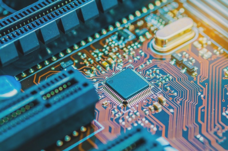
The fundamental testing principle of the PCB board light test machine follows Ohm’s law. It involves applying a specific test voltage between designated points, using a decoding circuit to select testing points on the PCB board, and determining the resistance value between these points. The voltage comparison circuit is used to test resistance or continuity between points, with the entire circuit board evaluated through this process.

Hardware Control System Overview
The test process involves controlling the test circuit to activate different test switches under the direction of the host computer. The system comprises the upper computer PC104, test control logic (implemented by FPGA), and high-voltage test circuit. The FPGA controls the high-voltage test circuit for PCB board testing, with the PC104 serving as the upper computer for human-computer interaction and control output.
Interface Circuits
The interface circuit between FPGA and PC104 utilizes the PC104 bus for communication, with the FPGA controlling the test circuit through this bus. Additionally, the interface between FPGA and Serial A/D and D/A devices involves using devices like TLC2543 and TLV5618 for A/D and D/A conversion, respectively, to meet system design requirements.
FPGA Programming Framework
The Importance of On-Chip FPGA Programming in PCB Testing Systems
- Utilizing the top-down FPGA design principle, a PCB testing system is divided into 5 key modules:
- Communication Module (ISA)
- Test Module (TEST)
- AD/DA Module
- Decoding Module (DECODER)
- RAM Control Module (RAMCTL)
- The ISA module handles system communication and control, interpreting command words, and generating control signals.
- The AD/DA module outputs reference voltage based on host computer parameters and conducts test procedures.
- The RAM control module facilitates data sharing between modules by reading and writing to RAM.
- The test module follows standard procedures and saves results in RAM.
- The decoding module maps switch numbers to circuits, enabling test switch information usage.
- The AD/DA module designs the SPI bus interface for A/D and D/A devices.
- Modules are written in Verilog, simulated using Modelsim and QuartusII.
- Altera’s IP core optimizes program modules, enhancing system design.
- Hardware control system, based on FPGA, boosts testing speed and simplifies circuit design.
By employing FPGA programming in PCB testing systems, both software and hardware optimization are achievable, paving the way for system upgrades and enhanced performance.