The Essential Guide to High-Speed PCB Signal Line Routing
1. Optimal Layer Count Selection
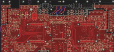
High-speed PCBs require careful consideration of layer count to minimize interference, improve grounding, and reduce signal degradation. Research shows that noise levels can be significantly lower on multilayer boards compared to double-sided boards.
2. Lead Bend Reduction
Keeping lead bends between high-speed circuit component pins as straight as possible or using 45° angles can minimize external radiation and signal coupling.
3. Lead Length Minimization
Reducing the distance between pins in high-frequency circuits helps to maintain signal integrity and performance. Prioritizing critical signal routing is key.
4. Via Usage Optimization
Minimizing via usage in component connections reduces distributed capacitance, leading to improved signal speed and overall PCB performance.
5. Cross Interference Management
When routing signal lines in parallel, consider using ground traces to reduce interference. Proper routing directions and ground plane placement are crucial for high-frequency circuit designs.
6. Ground Plane Shielding
Implement shielding for sensitive signal lines and critical components to ensure the stability of high-speed systems.
7. Loop-Free Signal Routing
Avoid creating loops or current loops in signal routing to maintain signal integrity.
8. Decoupling Capacitor Placement
Place high-frequency decoupling capacitors near integrated circuit blocks to enhance system stability.
Ground Wire Design Tips
Proper grounding is essential for controlling interference in electronic systems. Consider single-point and multi-point grounding based on signal frequencies and impedance levels.
PCB Design Best Practices
- Separate Digital and Analog Grounds
- Increase Ground Trace Width
- Use Closed Ground Loops for Digital Circuits
It’s essential to physically separate high-speed digital circuits and analog circuits on the same PCB. Avoid sharing ground traces and connect them to separate power supply grounds. Maximizing the grounding area for analog circuits helps minimize noise coupling.
Thin ground traces can lead to voltage fluctuations and unstable timing signals. To improve noise immunity, ensure ground traces are thick enough to handle current changes. A ground trace width of at least 3mm is recommended to support 3 times the maximum allowable current for the PCB.
For PCBs with digital circuits, a closed-loop ground design is beneficial. This design enhances noise immunity by reducing potential differences across the ground plane. It is especially useful in designs with multiple integrated circuits or power-hungry components, minimizing ground bounce and improving noise resistance.
If you have any questions about PCB design, feel free to contact us at info@wellcircuits.com.