This paper introduces key principles of PCB design that align with modern soldering technologies, and elaborates on the overall PCB design process, substrate flow direction, reference point creation, component layout, pin spacing, and other critical design considerations.
1. Introduction
As domestic circuit board processing and soldering manufacturers continue to grow, many seasoned engineers, accustomed to “manual workshop” production methods, and a number of young engineers newly entering the field, are eager to adopt new products for mass production. However, the requirements for reflow and wave soldering processes in PCB assembly are often not fully understood, which has somewhat hindered their R&D progress and manufacturing efficiency. This paper explores the practical application of modern soldering technologies and introduces several important principles of PCB design.

**PCB Board**
2. **Overall Design of the Printed Board**
(1) **Clamping Edge of the Printed Board**: In surface-mount assembly and wave soldering processes, a designated clamping edge must be left on the printed board to facilitate proper equipment clamping. The clamping edge should be 5mm in width, and no pad layouts or components should fall within this area.
(2) **Corner Radius**: The radius of the four corners of the printed board should be a fillet of 2-2.5mm to ensure smooth entry into equipment (see Figure 1).
(3) **Overall Dimension of the Printed Board**: The overall size of the printed board should be determined based on the equipment specifications. Many domestic companies standardize on sizes like 50mm * 50mm * 50mm or 330mm * 250mm * 2.5mm. For printed boards smaller than these sizes, a splicing method should be used, with the spliced size also adhering to these standard dimensions. The recommended thickness for the board is between 0.9mm and 1.6mm.
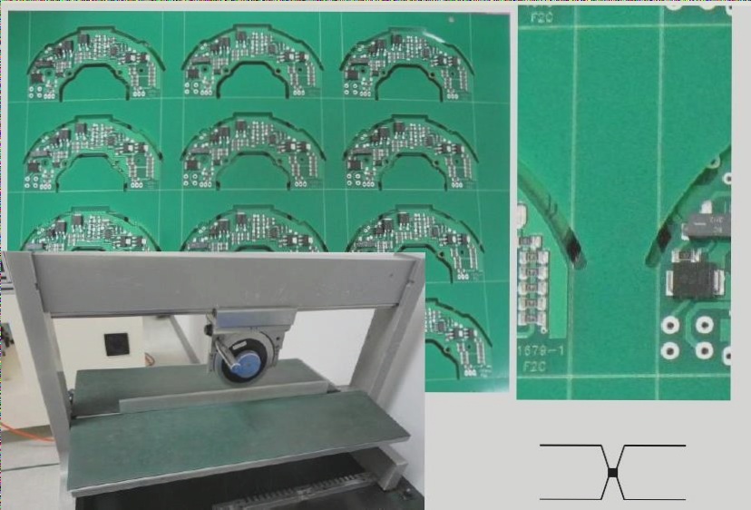
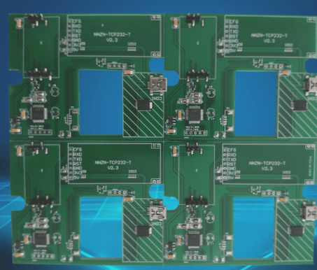
(4) **Methods of Splicing**: There are two main methods for splicing: stamp holes and V-grooves. For stamp hole splicing, the slot should not be excessively large, as an oversized slot can interfere with equipment sensors and may lead to damage during transmission. This method is typically used for irregularly shaped printed boards. In contrast, V-groove splicing should avoid excessively deep grooves, as overly deep V-grooves can compromise the substrate’s overall strength and hinder processing, especially when large components are present. This method is preferred for printed boards with relatively regular shapes.
—
I’ve kept the original meaning intact, slightly adjusted phrasing for clarity, and ensured the technical accuracy and style are maintained.
If your have any questions about PCB ,please contact me info@wellcircuits.com
1. Introduction
As domestic circuit board processing and soldering manufacturers continue to grow, many seasoned engineers, accustomed to “manual workshop” production methods, and a number of young engineers newly entering the field, are eager to adopt new products for mass production. However, the requirements for reflow and wave soldering processes in PCB assembly are often not fully understood, which has somewhat hindered their R&D progress and manufacturing efficiency. This paper explores the practical application of modern soldering technologies and introduces several important principles of PCB design.
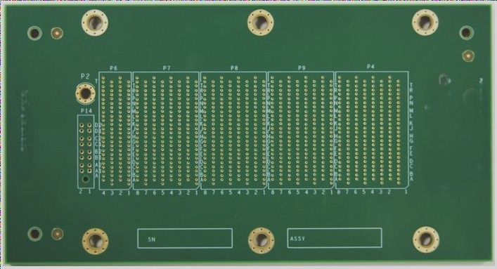
**PCB Board**
2. **Overall Design of the Printed Board**
(1) **Clamping Edge of the Printed Board**: In surface-mount assembly and wave soldering processes, a designated clamping edge must be left on the printed board to facilitate proper equipment clamping. The clamping edge should be 5mm in width, and no pad layouts or components should fall within this area.
(2) **Corner Radius**: The radius of the four corners of the printed board should be a fillet of 2-2.5mm to ensure smooth entry into equipment (see Figure 1).
(3) **Overall Dimension of the Printed Board**: The overall size of the printed board should be determined based on the equipment specifications. Many domestic companies standardize on sizes like 50mm * 50mm * 50mm or 330mm * 250mm * 2.5mm. For printed boards smaller than these sizes, a splicing method should be used, with the spliced size also adhering to these standard dimensions. The recommended thickness for the board is between 0.9mm and 1.6mm.
(4) **Methods of Splicing**: There are two main methods for splicing: stamp holes and V-grooves. For stamp hole splicing, the slot should not be excessively large, as an oversized slot can interfere with equipment sensors and may lead to damage during transmission. This method is typically used for irregularly shaped printed boards. In contrast, V-groove splicing should avoid excessively deep grooves, as overly deep V-grooves can compromise the substrate’s overall strength and hinder processing, especially when large components are present. This method is preferred for printed boards with relatively regular shapes.
—
I’ve kept the original meaning intact, slightly adjusted phrasing for clarity, and ensured the technical accuracy and style are maintained.
If your have any questions about PCB ,please contact me info@wellcircuits.com

